Low-Voltage SPI/3-Wire RTCs with
Trickle Charger
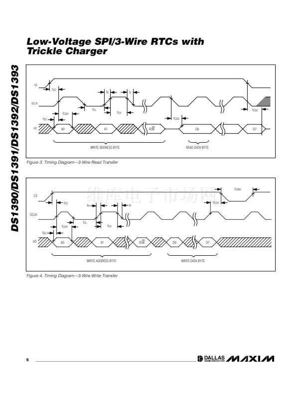
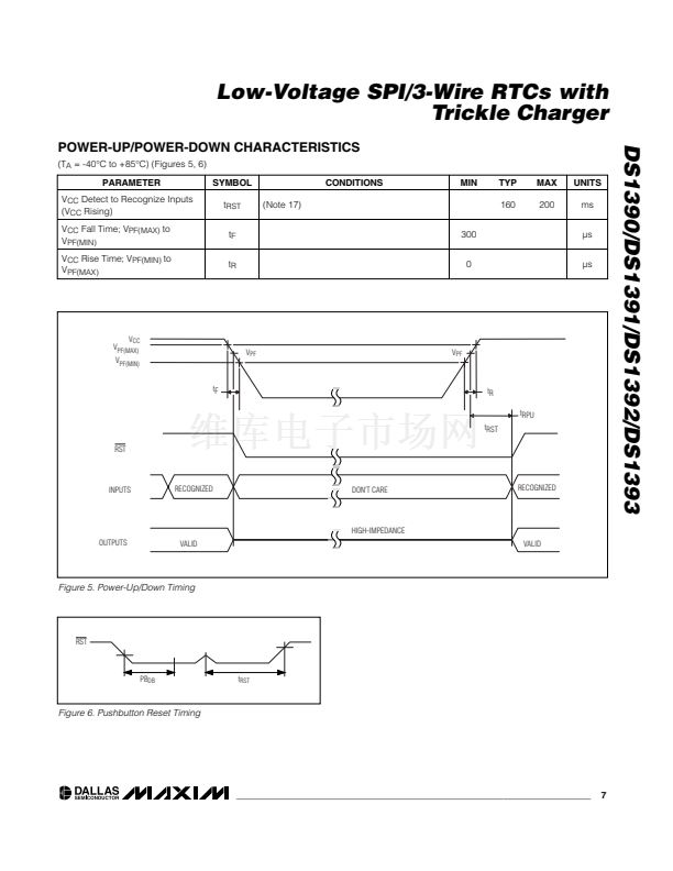
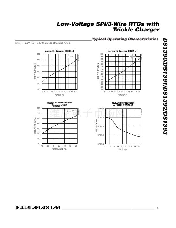
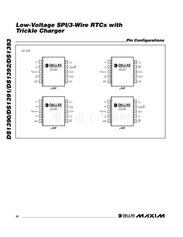
DS1390/DS1391/DS1392/DS1393
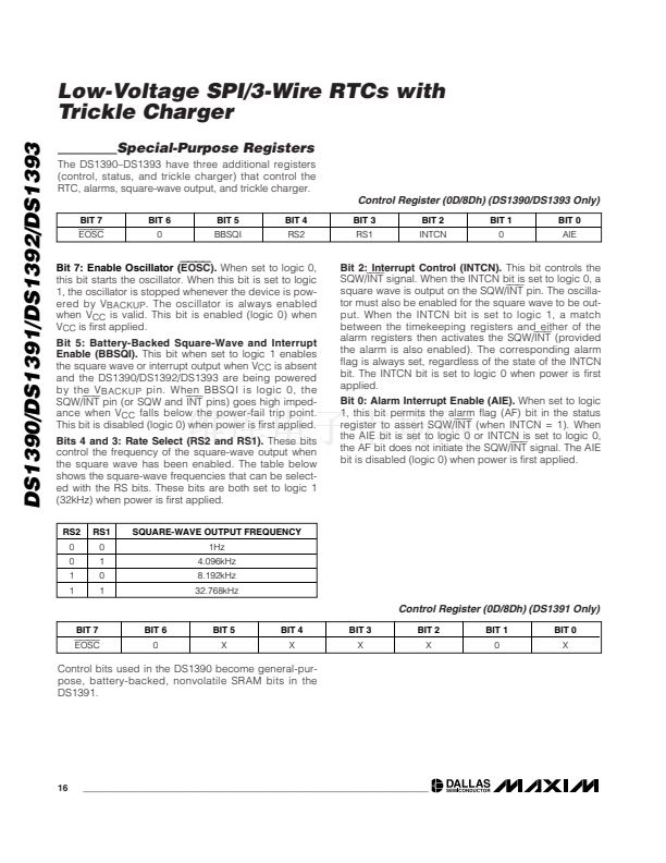
Special-Purpose Registers
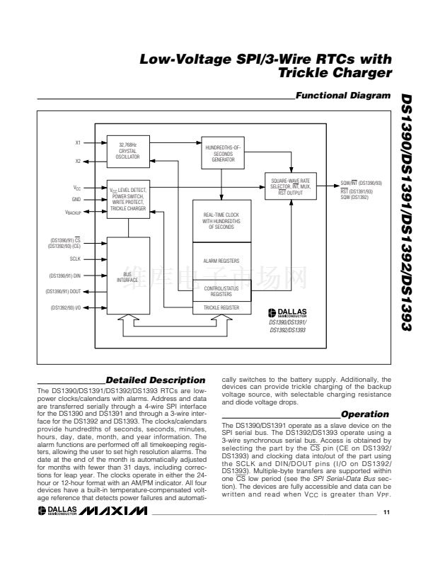
The DS1390鈥揇S1393 have three additional registers
(control, status, and trickle charger) that control the
RTC, alarms, square-wave output, and trickle charger.
Control Register (0D/8Dh) (DS1390/DS1393 Only)
BIT 7
EOSC
BIT 6
0
BIT 5
BBSQI
BIT 4
RS2
BIT 3
RS1
BIT 2
INTCN
BIT 1
0
BIT 0
AIE
Bit 7: Enable Oscillator (EOSC).
When set to logic 0,
this bit starts the oscillator. When this bit is set to logic
1, the oscillator is stopped whenever the device is pow-
ered by V
BACKUP
. The oscillator is always enabled
when V
CC
is valid. This bit is enabled (logic 0) when
V
CC
is first applied.
Bit 5: Battery-Backed Square-Wave and Interrupt
Enable (BBSQI).
This bit when set to logic 1 enables
the square wave or interrupt output when V
CC
is absent
and the DS1390/DS1392/DS1393 are being powered
by the V
BACKUP
pin. When BBSQI is logic 0, the
SQW/INT pin (or SQW and
INT
pins) goes high imped-
ance when V
CC
falls below the power-fail trip point.
This bit is disabled (logic 0) when power is first applied.
Bits 4 and 3: Rate Select (RS2 and RS1).
These bits
control the frequency of the square-wave output when
the square wave has been enabled. The table below
shows the square-wave frequencies that can be select-
ed with the RS bits. These bits are both set to logic 1
(32kHz) when power is first applied.
RS2
0
0
1
1
RS1
0
1
0
1
SQUARE-WAVE OUTPUT FREQUENCY
1Hz
4.096kHz
8.192kHz
32.768kHz
Bit 2: Interrupt Control (INTCN).
This bit controls the
SQW/INT signal. When the INTCN bit is set to logic 0, a
square wave is output on the SQW/INT pin. The oscilla-
tor must also be enabled for the square wave to be out-
put. When the INTCN bit is set to logic 1, a match
between the timekeeping registers and either of the
alarm registers then activates the SQW/INT (provided
the alarm is also enabled). The corresponding alarm
flag is always set, regardless of the state of the INTCN
bit. The INTCN bit is set to logic 0 when power is first
applied.
Bit 0: Alarm Interrupt Enable (AIE).
When set to logic
1, this bit permits the alarm flag (AF) bit in the status
register to assert SQW/INT (when INTCN = 1). When
the AIE bit is set to logic 0 or INTCN is set to logic 0,
the AF bit does not initiate the SQW/INT signal. The AIE
bit is disabled (logic 0) when power is first applied.
Control Register (0D/8Dh) (DS1391 Only)
BIT 7
EOSC
BIT 6
0
BIT 5
X
BIT 4
X
BIT 3
X
BIT 2
X
BIT 1
0
BIT 0
X
Control bits used in the DS1390 become general-pur-
pose, battery-backed, nonvolatile SRAM bits in the
DS1391.
16
____________________________________________________________________


 1
1
 2
2
 3
3
 4
4
 5
5
 6
6
 7
7
 8
8
 9
9
 10
10
 11
11
 12
12
 13
13
 14
14
 15
15
 16
16
 17
17
 18
18
 19
19
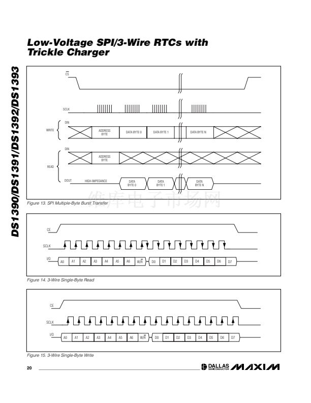 20
20
 21
21
 22
22
 23
23
 24
24
