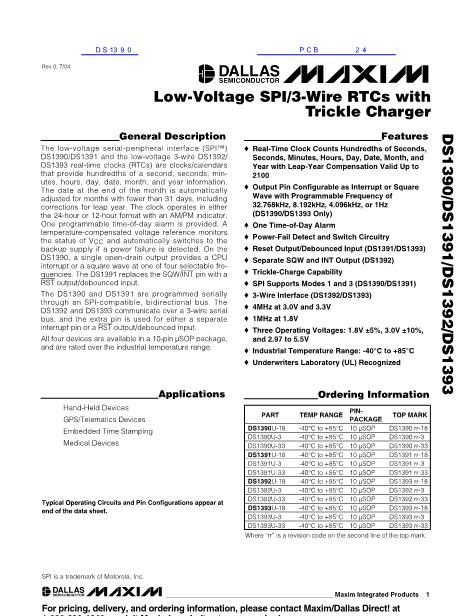
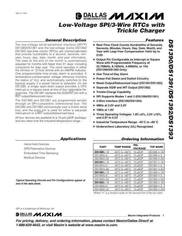
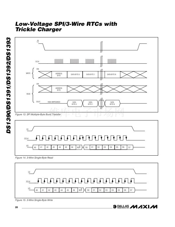
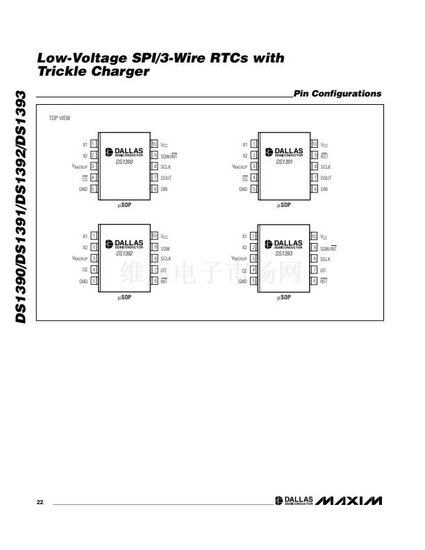
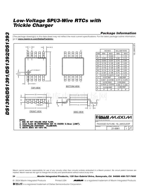
Low-Voltage SPI/3-Wire RTCs with
Trickle Charger
DS1390/DS1391/DS1392/DS1393
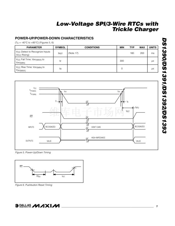
However, when V
CC
falls below V
PF
, the internal clock
registers are blocked from any access. If V
PF
is less
than V
BACKUP
, the device power is switched from V
CC
to V
BACKUP
when V
CC
drops below V
PF
. If V
PF
is
greater than V
BACKUP
, the device power is switched
from V
CC
to V
BACKUP
when V
CC
drops below
V
BACKUP
. The registers are maintained from the
V
BACKUP
source until V
CC
is returned to nominal levels.
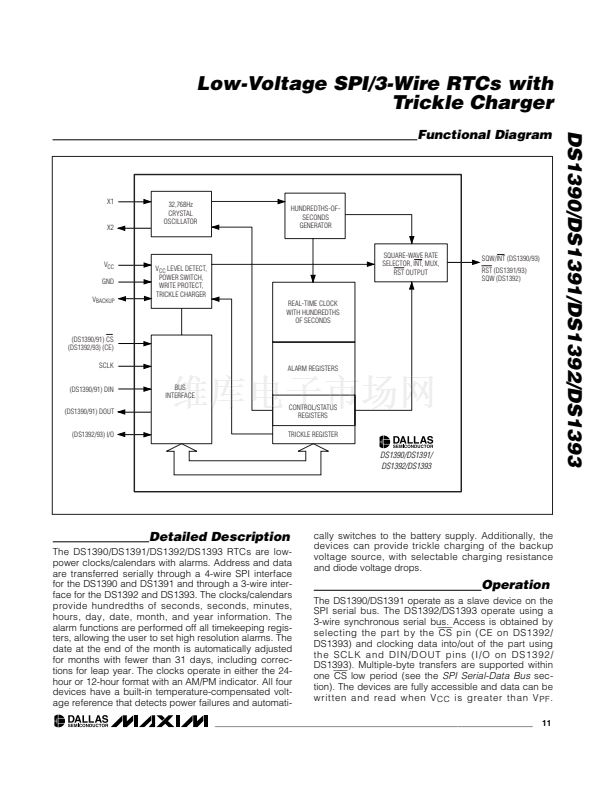
See the
Functional Diagram
for the main elements of
these serial RTCs.
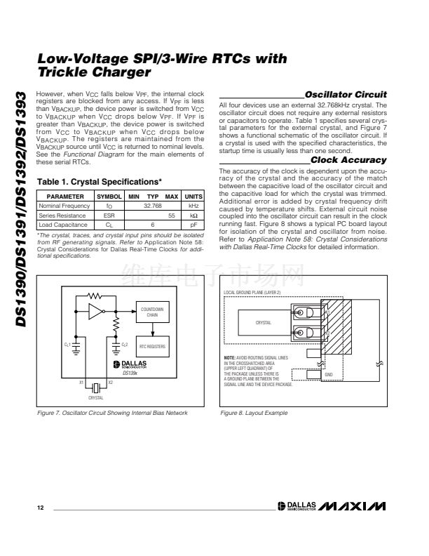
Oscillator Circuit
All four devices use an external 32.768kHz crystal. The
oscillator circuit does not require any external resistors
or capacitors to operate. Table 1 specifies several crys-
tal parameters for the external crystal, and Figure 7
shows a functional schematic of the oscillator circuit. If
a crystal is used with the specified characteristics, the
startup time is usually less than one second.
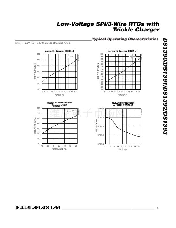
Clock Accuracy
The accuracy of the clock is dependent upon the accu-
racy of the crystal and the accuracy of the match
between the capacitive load of the oscillator circuit and
the capacitive load for which the crystal was trimmed.
Additional error is added by crystal frequency drift
caused by temperature shifts. External circuit noise
coupled into the oscillator circuit can result in the clock
running fast. Figure 8 shows a typical PC board layout
for isolation of the crystal and oscillator from noise.
Refer to
Application Note 58: Crystal Considerations
with Dallas Real-Time Clocks
for detailed information.
Table 1. Crystal Specifications*
PARAMETER
Nominal Frequency
Series Resistance
Load Capacitance
SYMBOL
f
O
ESR
C
L
6
MIN
TYP
32.768
55
MAX
UNITS
kHz
k鈩?/div>
pF
*The
crystal, traces, and crystal input pins should be isolated
from RF generating signals. Refer to
Application Note 58:
Crystal Considerations for Dallas Real-Time Clocks
for addi-
tional specifications.
LOCAL GROUND PLANE (LAYER 2)
COUNTDOWN
CHAIN
X1
CRYSTAL
X2
C
L
1
C
L
2
RTC REGISTERS
DS139x
X1
X2
NOTE:
AVOID ROUTING SIGNAL LINES
IN THE CROSSHATCHED AREA
(UPPER LEFT QUADRANT) OF
THE PACKAGE UNLESS THERE IS
A GROUND PLANE BETWEEN THE
SIGNAL LINE AND THE DEVICE PACKAGE.
GND
CRYSTAL
Figure 7. Oscillator Circuit Showing Internal Bias Network
Figure 8. Layout Example
12
____________________________________________________________________


 1
1
 2
2
 3
3
 4
4
 5
5
 6
6
 7
7
 8
8
 9
9
 10
10
 11
11
 12
12
 13
13
 14
14
 15
15
 16
16
 17
17
 18
18
 19
19
 20
20
 21
21
 22
22
 23
23
 24
24
