鈮?/div>
85擄C, unless otherwise specified.
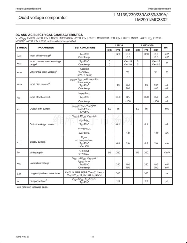
SYMBOL
V
OS
V
CM
V
IDR
PARAMETER
Input offset voltage
2
Input common鈥搈ode voltage
range
3
Differential input
voltage
1
TEST CONDITIONS
T
A
=25擄C
Over temp.
T
A
=25擄C
Over temp.
Keep all
V
INs
鈮?V
DC
(or V鈥?if need)
I
IN(+)
or I
IN(鈥?
with output in
linear range
T
A
=25擄C
Over temp.
I
IN(+)
鈥揑
IN(鈥?
I
OS
Input offset current
T
A
=25擄C
Over temp.
I
OL
Output sink current
V
IN(鈥?
鈮?V
DC
, V
IN
(+)=0,
V
O
鈮?.5V
DC
,
T
A
=25擄C
V
IN(+)
鈮?V
DC
, V
IN
(鈥?=0
V
O
=5V
DC
,
Output leakage current
T
A
=25擄C
V
O
=30V
DC
,
over temp.
R
L
=鈭?on all comparators,
I
CC
Supply current
T
A
=25擄C
R
L
=鈭?on all comparators, V+=30V
A
V
Voltage gain
R
L
鈮?5k鈩?
V+=15V
DC
V
IN(鈥?
鈮?V
DC
, V
IN(+)
=0,
I
SINK
鈮?mA
T
A
=25擄C
Over temp.
V
IN
=TTL logic swing, V
REF
=1.4V
DC
,
V
RL
=5V
DC
, R
L
=5.1k鈩? T
A
=25擄C
V
RL
=5V
DC
, R
L
=5.1k鈩?
T
A
=25擄C
25
0.8
1.0
100
2.0
2.5
2
100
mA
V/mV
1.0
.8
1.0
1.8
碌A(chǔ)
mA
0.1
0.1
nA
6.0
鹵5
鹵50
16
鹵50
鹵200
6
16
mA
鹵5
鹵100
鹵300
nA
nA
0
0
LM2901
Min
Typ
鹵2.0
鹵9
Max
鹵7.0
鹵15
V+鈥?.5
V+鈥?.0
V+
0
0
Min
MC3302
Typ
鹵3.0
Max
鹵20
鹵40
V+鈥?.5
V+鈥?.0
V+
UNIT
mV
mV
V
V
I
BIAS
Input bias current
4
25
200
250
500
25
500
1000
nA
nA
V
OL
Saturation voltage
400
300
1.3
400
700
150
400
700
mV
mV
ns
碌s
t
LSR
t
R
Large鈥搒ignal response time
Response time
5
300
1.3
NOTES:
1. Positive excursions of input voltage may exceed the power supply level by 17V. As long as the other voltage remains within the
common-mode range, the comparator will provide a proper output state. The low input voltage state must not be less than 鈥?.3V
DC
(or
0.3V
DC
below the magnitude of the negative power supply, if used).
2. At output switch point, V
O
鈮?/div>
1.4V
DC
, R
S
=0鈩?with V+ from 5V
DC
to 30V
DC
; and over the full input common鈥搈ode range (0V
DC
to
V+ 鈥?1.5V
DC
). Inputs of unused comparators should be grounded.
3. The input common鈥搈ode voltage or either input signal voltage should not be allowed to go negative by more than 0.3V. The upper end of
the common鈥搈ode voltage range is V+ 鈥?1.5V, but either or both inputs can go to 30V
DC
without damage.
4. The direction of the input current is out of the IC due to the PNP input stage. This current is essentially constant, independent of the state of
the output so no loading change exists on the reference or input lines.
5. The response time specified is for a 100mV input step with a 5mV overdrive. For larger overdrive signals, 300ns can be obtained (see typical
performance characteristics section).
1995 Nov 27
6


 1
1
 2
2
 3
3
 4
4
 5
5
 6
6
 7
7
 8
8
 9
9
 10
10
