鈥?/div>
Synchronizes to clock-and-sync-pair to maintain
minimal phase skew between the master-clock
and the redundant slave-clock
Supports ITU-T G.813 option 1, G.823 for 2048 kbs
and G.824 for 1544 kbs interfaces
Supports Telcordia GR-1244-CORE Stratum
3/4/4E
Supports ANSI T1.403 and ETSI ETS 300 011 for
ISDN primary rate interfaces
Accepts three input references and synchronizes
to any combination of 2 kHz, 8 kHz, 1.544 MHz,
2.048 MHz, 8.192 MHz, 16.384 MHz or 19.44 MHz
inputs
Provides a range of clock outputs: 1.544 MHz
(DS1), 2.048 MHz (E1), 3.088 MHz, 16.384 MHz,
and 19.44 MHz (SDH), and either 4.096 MHz and
8.192 MHz or 32.768 MHz and 65.536 MHz, and a
choice of 6.312 MHz (DS2), 8.448 MHz (E2),
44.736 MHz (DS3) or 34.368 MHz (E3)
Provides 5 styles of 8 kHz framing pulses and a
2 kHz multi-frame pulse
Holdover frequency accuracy of 1x10
-8
Selectable loop filter 1.8 Hz, 3.6 Hz or 922 Hz
Less than 20 ps
rms
intrinsic jitter on the 19.44 MHz
output clock, compliant with GR-253-CORE OC-3
and G.813 STM-1 specifications
OSCi
OSCo
TIE_CLR
June 2004
Ordering Information
ZL30105QDG
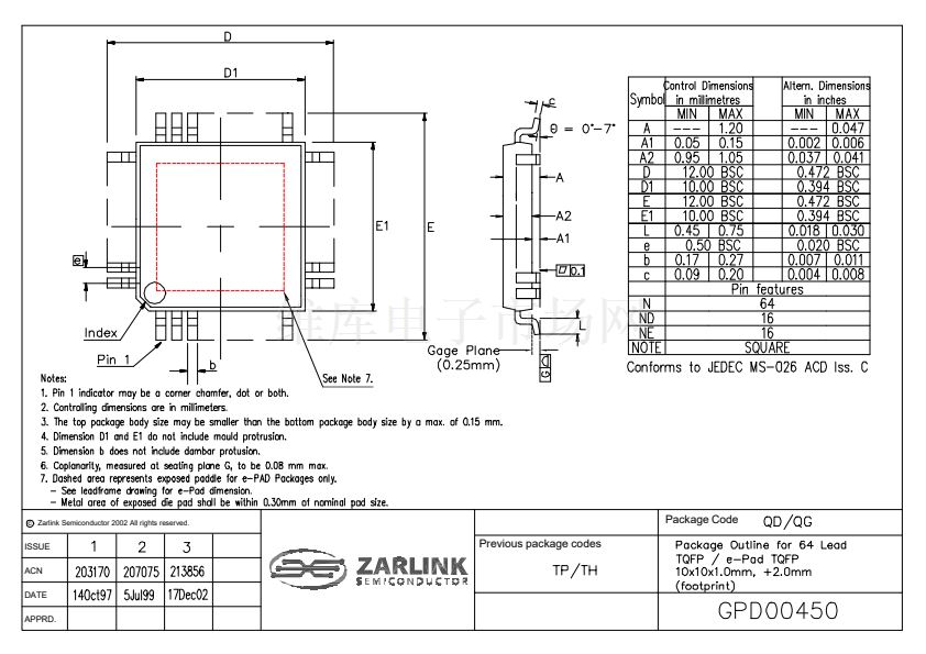
64 pin TQFP
鈥?/div>
鈥?/div>
鈥?/div>
鈥?/div>
-40擄C to +85擄C
鈥?/div>
鈥?/div>
鈥?/div>
鈥?/div>
鈥?/div>
Less than 0.6 ns
pp
intrinsic jitter on all output
clocks and frame pulses
Manual or Automatic hitless reference switching
Provides Lock, Holdover and selectable Out of
Range indication
Simple hardware control interface
Selectable external master clock source: Clock
Oscillator or Crystal
鈥?/div>
Applications
鈥?/div>
Synchronization and timing control for multi-trunk
SDH and T1/E1 systems such as DSLAMs,
Gateways and PBXs
Clock and frame pulse source for
AdvancedTCA鈩? and other time division
multiplex (TDM) buses
鈥?/div>
鈥?/div>
鈥?/div>
鈥?/div>
鈥?/div>
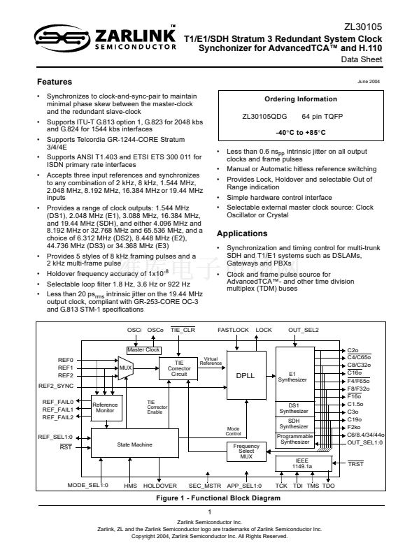
FASTLOCK
LOCK
OUT_SEL2
Master Clock
REF0
REF1
REF2
REF2_SYNC
REF_FAIL0
REF_FAIL1
REF_FAIL2
TIE
Corrector
Enable
MUX
TIE
Corrector
Circuit
Virtual
Reference
DPLL
E1
Synthesizer
Reference
Monitor
DS1
Synthesizer
Mode
Control
SDH
Synthesizer
Programmable
Synthesizer
REF_SEL1:0
RST
State Machine
Frequency
Select
MUX
C2o
C4/C65o
C8/C32o
C16o
F4/F65o
F8/F32o
F16o
C1.5o
C3o
C19o
F2ko
C6/8.4/34/44o
OUT_SEL1:0
IEEE
1149.1a
TRST
MODE_SEL1:0
HMS
HOLDOVER
SEC_MSTR
APP_SEL1:0
TCK
TDI TMS TDO
Figure 1 - Functional Block Diagram
1
Zarlink Semiconductor Inc.
Zarlink, ZL and the Zarlink Semiconductor logo are trademarks of Zarlink Semiconductor Inc.
Copyright 2004, Zarlink Semiconductor Inc. All Rights Reserved.
ZL30105QDG相關(guān)型號(hào)PDF文件下載
-
型號(hào)
版本
描述
廠商
下載
-
英文版
T1/E1 System Synchronizer
-
英文版
T1/E1 System Synchronizer
ZARLINK [Z...
-
英文版
T1/E1 Stratum 3 System Synchronizer
-
英文版
T1/E1 Stratum 3 System Synchronizer
ZARLINK [Z...
-
英文版
T1/E1 Stratum 4/4E Redundant System Clock Synchronizer for D...
-
英文版
T1/E1 Stratum 4/4E Redundant System Clock Synchronizer for D...
ZARLINK [Z...
-
英文版
T1/E1/SDH Stratum 3 Redundant System Clock Synchonizer for A...
-
英文版
T1/E1/SDH Stratum 3 Redundant System Clock Synchonizer for A...
ZARLINK [Z...
-
英文版
SONET/SDH/PDH Network Interface DPLL
-
英文版
SONET/SDH/PDH Network Interface DPLL
ZARLINK [Z...
-
英文版
GbE Line Card Synchronizer
ZARLINK [Z...
-
英文版
Network Interface DPLL
-
英文版
Network Interface DPLL
ZARLINK [Z...
-
英文版
DS1/E1 System Synchronizer with 19.44 MHz Output
-
英文版
DS1/E1 System Synchronizer with 19.44 MHz Output
ZARLINK [Z...
-
英文版
Telecom Rate Conversion DPLL
ZARLINK [Z...
-
英文版
POTS Line Card PLL
ZARLINK [Z...
-
英文版
SONET/SDH OC-48/OC-192 System Synchronizer
ZARLINK [Z...
-
英文版
SONET/SDH OC-48/OC-192 Line Card Synchronizer
ZARLINK [Z...
-
英文版
Low Jitter Line Card Synchronizer
ZARLINK [Z...


 1
1
 2
2
 3
3
 4
4
 5
5
 6
6
 7
7
 8
8
 9
9
 10
10
 11
11
 12
12
 13
13
 14
14
 15
15
 16
16
 17
17
 18
18
 19
19
 20
20
 21
21
 22
22
 23
23
 24
24
 25
25
 26
26
 27
27
 28
28
 29
29
 30
30
 31
31
 32
32
 33
33
 34
34
 35
35
 36
36
 37
37
 38
38
 39
39
 40
40
 41
41
 42
42
 43
43
 44
44
 45
45
 46
46
 47
47
 48
48
 49
49
 50
50
