APPLICATION NOTE
0
R
XCR3320: 320 Macrocell SRAM
CPLD
0
14*
DS033 (v1.1) February 10, 2000
Product Specification
nique is also what allows Xilinx to offer a true CPLD archi-
tecture in a high density device.
The Xilinx XCR3320 devices use the patented XPLA2
(eXtended Programmable Logic Array) architecture. This
architecture combines the best features of both PAL- and
PLA-type logic structures to deliver high speed and flexible
logic allocation that results in superior ability to make
design changes with fixed pinouts. The XPLA2 architecture
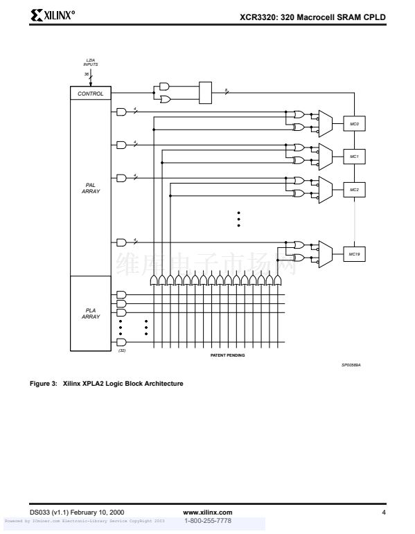
is constructed from 80 macrocell Fast Modules that are
connected together by an interconnect array. Within each
Fast Module are four Logic Blocks of 20 macrocells each.
Each Logic Block contains a PAL structure with four dedi-
cated product terms for each macrocell. In addition, each
Logic Block has 32 additional product terms in a PLA struc-
ture that can be shared through a fully programmable OR
array to any of the 20 macrocells. This combination effi-
ciently allocates logic throughout the Logic Block, which
increases device density and allows for design changes
without re-defining the pinout or changing the system tim-
ing. The XCR3320 offers pin-to-pin propagation delays of
7.5 ns through the PAL array of a Fast Module; and if the
PLA array is used, an additional 1.5 ns is added to the
delay, no matter how many PLA product terms are used. If
the interconnect array between Fast Modules is used, there
is a second fixed delay of 2.0 ns. This means that the worst
case pin-to-pin propagation delay within a fast module is
7.5 + 1.5 = 9.0 ns, and the delay from any pin to any other
pin across the entire chip is 7.5 + 2.0 = 9.5 ns if only the
PAL array is used, and 7.5 + 1.5 + 2.0 = 11.0 ns if the PLA
array is used.
Each macrocell also has a two input XOR gate with the
dedicated PAL product terms on one input and the PLA
product terms on the other input. This patent-pending Ver-
satile XOR structure allows for very efficient logic optimiza-
tion compared to competing XOR structures that have only
one product term as the second input to the XOR gate. The
Versatile XOR allows an 8-bit XOR function to be imple-
mented in only 20 product terms, compared to 65 product
terms for the traditional XOR approach.
The XCR3320 is SRAM-based, which means that it is con-
figured from an external source at power up. See the con-
figuration section of this data sheet for more information.
The device supports the full JTAG specification (IEEE
1149.1) through an industry standard JTAG interface. It can
also be configured through the JTAG port, which is very
useful for prototyping. See section titled
鈥淒evice Configura-
tion Through JTAG鈥?on page 29
for more information.
Features
鈥?/div>
鈥?/div>
鈥?/div>
320 macrocell SRAM based CPLD
Configuration times of under 1.0 second
IEEE 1149.1 compliant JTAG testing capability
- Five pin JTAG interface
- IEEE 1149.1 TAP controller
In system configurable
3.3V device with 5V tolerant I/O
Innovative XPLA2 Architecture combines extreme
flexibility and high speeds
Eight synchronous clock networks with programmable
polarity at every macrocell
Up to 32 asynchronous clocks support complex
clocking needs
Innovative XOR structure at every macrocell provides
excellent logic reduction capability
Logic expandable to 36 product terms on a single
macrocell
Advanced 0.35碌 SRAM process
Design entry and verification using industry standard
and Xilinx CAE tools
Control Term structure provides either sum terms or
product terms in each logic block for:
- 3-state buffer control
- Asynchronous macrocell register reset/preset
Global 3-state pin facilitates "bed of nails" testing
without sacrificing logic resources
Programmable slew rate control
Small form factor packages with high I/O counts
Available in commercial and industrial temperature
ranges
鈥?/div>
鈥?/div>
鈥?/div>
鈥?/div>
鈥?/div>
鈥?/div>
鈥?/div>
鈥?/div>
鈥?/div>
鈥?/div>
鈥?/div>
鈥?/div>
鈥?/div>
鈥?/div>
Description
The XCR3320 device is a member of the CoolRunner鈩?/div>
family of high-density SRAM-based CPLDs (Complex Pro-
grammable Logic Device) from Xilinx. This device com-
bines high speed and deterministic pin-to-pin timing with
high density. The XCR3320 uses the patented Fast Zero
Power (FZP鈩? design technique that combines high speed
and low power for the first time ever in a CPLD. FZP allows
the XCR3320 to have true pin-to-pin timing delays of 7.5 ns,
and standby currents of 100
碌A(chǔ)
without the need for `turbo
bits' or other power down schemes. By replacing conven-
tional sense amplifier methods for implementing product
terms (a technique that has been used since the bipolar
era) with a cascaded chain of pure CMOS gates, both
standby and dynamic power are dramatically reduced
when compared to other CPLDs. The FZP design tech-
DS033 (v1.1) February 10, 2000
Powered by ICminer.com Electronic-Library Service CopyRight 2003
www.xilinx.com
1-800-255-7778
1
XCR3320-10TQ144C相關(guān)型號PDF文件下載
-
型號
版本
描述
廠商
下載
-
英文版
32 Macrocell CPLD
XILINX [Xi...
-
英文版
Product Specification
-
英文版
Product Specification
-
英文版
Product Specification
-
英文版
Product Specification
-
英文版
with Enhanced Clocking
-
英文版
64 Macrocell CPLD With Enhanced Clocking
XILINX [Xi...
-
英文版
CPLD with Enhanced Clocking
-
英文版
CPLD with Enhanced Clocking
XILINX [Xi...
-
英文版
XCR3032XL 32 Macrocell CPLD
-
英文版
XCR3032XL 32 Macrocell CPLD
XILINX [Xi...
-
英文版
XCR3064XL 64 Macrocell CPLD
-
英文版
XCR3064XL 64 Macrocell CPLD
XILINX [Xi...
-
英文版
XCR3128XL 128 Macrocell CPLD
-
英文版
XCR3128XL 128 Macrocell CPLD
XILINX [Xi...
-
英文版
256 Macrocell CPLD
-
英文版
256 Macrocell CPLD
XILINX [Xi...
-
英文版
256 Macrocell CPLD
XILINX [Xi...
-
英文版
384 Macrocell CPLD
-
英文版
384 Macrocell CPLD
XILINX [Xi...


 1
1
 2
2
 3
3
 4
4
 5
5
 6
6
 7
7
 8
8
 9
9
 10
10
 11
11
 12
12
 13
13
 14
14
 15
15
 16
16
 17
17
 18
18
 19
19
 20
20
 21
21
 22
22
 23
23
 24
24
 25
25
 26
26
 27
27
 28
28
 29
29
 30
30
 31
31
 32
32
 33
33
 34
34
 35
35
 36
36
 37
37
 38
38
 39
39
 40
40
 41
41
 42
42
 43
43
