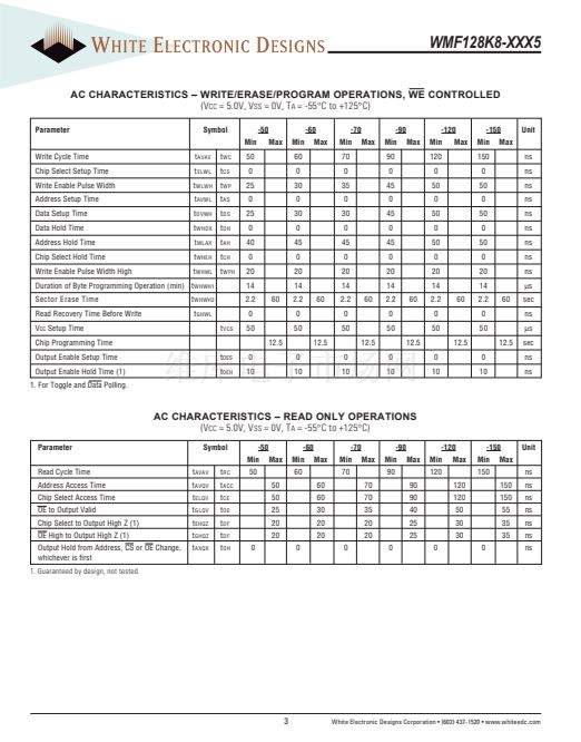
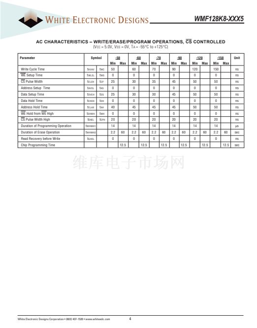
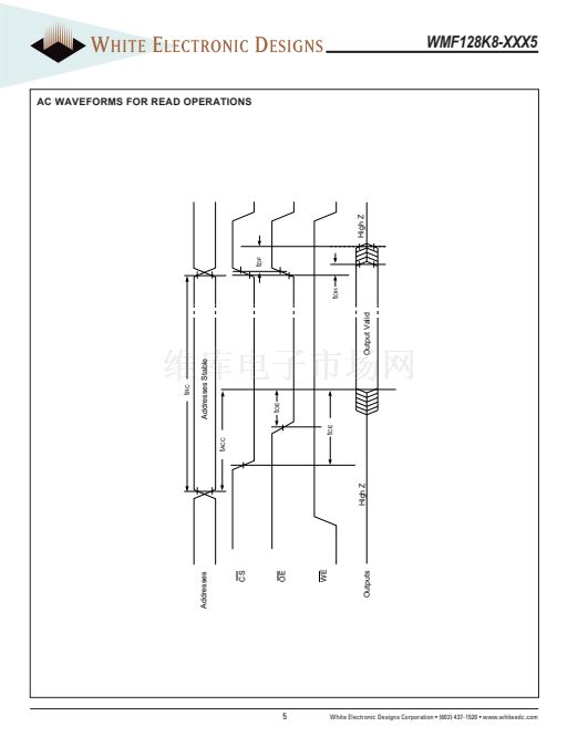
WMF128K8-XXX5
HI-RELIABILITY PRODUCT
128Kx8 MONOLITHIC FLASH, SMD 5962-96690
FEATURES
s
Access Times of 50*, 60, 70, 90, 120, 150ns
s
Packaging
鈥?32 lead, Hermetic Ceramic, 0.400" SOJ (Package 101)
鈥?32 pin, Hermetic Ceramic, 0.600" DIP (Package 300)
鈥?32 lead, Flatpack (Package 220)
鈥?32 lead, Formed Flatpack (Package 221)
鈥?32 pin, Rectangular Ceramic Leadless Chip Carrier
(Package 601)
s
100,000 Erase/Program Cycles Minimum
s
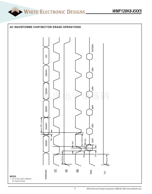
Sector Erase Architecture
鈥?8 equal size sectors of 16KBytes each
鈥?Any combination of sectors can be concurrently
erased. Also supports full chip erase
s
Organized as 128Kx8
s
Commercial, Industrial and Military Temperature Ranges
s
5 Volt Programming. 5V
鹵
10% Supply.
s
Low Power CMOS
s
Embedded Erase and Program Algorithms
s
TTL Compatible Inputs and CMOS Outputs
s
Page Program Operation and Internal Program Control Time.
Note: For programming information refer to Flash Programming 1M5
Application Note.
* The access time of 50ns is available in Industrial and Commercial
temperature ranges only.
PIN CONFIGURATION FOR WMF128K8-XXX5
32 DIP
32 CSOJ
32 FLATPACK
PIN CONFIGURATION FOR WMF128K8-XCLX5
32 CLCC
TOP VIEW
A12
NC
A16
A15
A12
A7
A6
A5
A4
A3
A2
A1
A0
I/O0
I/O1
I/O2
V
SS
TOP VIEW
A15
A16
V
CC
WE
NC
V
CC
WE
NC
A14
A13
A8
A9
A11
OE
A10
CS
I/O7
I/O6
I/O5
I/O4
I/O3
1
2
3
4
5
6
7
8
9
10
11
12
13
14
15
16
32
31
30
29
28
27
26
25
24
23
22
21
20
19
18
17
4 3 2 1 32 31 30
A7
A6
A5
A4
A3
A2
A1
A0
I/O
0
5
29
6
28
7
27
8
26
9
25
10
24
11
23
12
22
13
21
14 15 16 17 18 19 20
A14
A13
A8
A9
A11
OE
A10
CS
I/O7
I/O1
I/O2
I/O3
I/O4
I/O5
PIN DESCRIPTION
A
0
-
16
I/O
0-7
CS
OE
WE
V
CC
V
SS
Address Inputs
Data Input/Output
Chip Select
Output Enable
Write Enable
+5.0V Power
Ground
April 2001 Rev. 5
1
White Electronic Designs Corporation 鈥?(602) 437-1520 鈥?www.whiteedc.com
I/O6
V
SS
NC


 1
1
 2
2
 3
3
 4
4
 5
5
 6
6
 7
7
 8
8
 9
9
 10
10
 11
11
 12
12
 13
13
 14
14
