White Electronic Designs
8Mx32 SDRAM
FEATURES
n
n
n
n
n
n
n
53% Space Savings vs. Monolithic Solution
Reduced System Inductance and Capacitance
Pinout and Footprint Compatible to SSRAM 119 BGA
3.3V Operating Supply Voltage
Fully Synchronous to Positive Clock Edge
Clock Frequencies of 133MHz, 125MHz and 100MHz
Burst Operation
聲 Sequential or Interleave
聲 Burst Length = Programmable 1, 2, 4, 8 or Full Page
聲 Burst Read and Write
聲 Multiple Burst Read and Single Write
WED3DL328V
DESCRIPTION
The WED3DL328V is an 8Mx32 Synchronous DRAM
configured as 4x2Mx32. The SDRAM BGA is con-
structed with two 8Mx16 SDRAM die mounted on a
multi-layer laminate substrate and packaged in a 119
lead, 14mm by 22mm, BGA.
The WED3DL328V is an ideal SDRAM wide I/O memory
solution for all high performance, computer applica-
tions which include Network Processors, DSPs and
Functional ASICs.
The WED3DL328V is available in clock speeds of
133MHz, 125MHz and 100MHz. The range of operat-
ing frequencies, programmable burst lengths and
programmable latencies allow the same device to be
useful for a variety of high bandwidth, high performance
memory system applications.
The package and design provides performance en-
hancements via a 50% reduction in capacitance vs.
two monolithic devices. The design includes internal
ground and power planes which reduces inductance
on the ground and power pins allowing for improved
decoupling and a reduction in system noise.
n
n
n
n
n
Data Mask Control Per Byte
Auto and Self Refresh
Automatic and Controlled Precharge Commands
Suspend Mode and Power Down Mode
119 Pin BGA, JEDEC MO-163
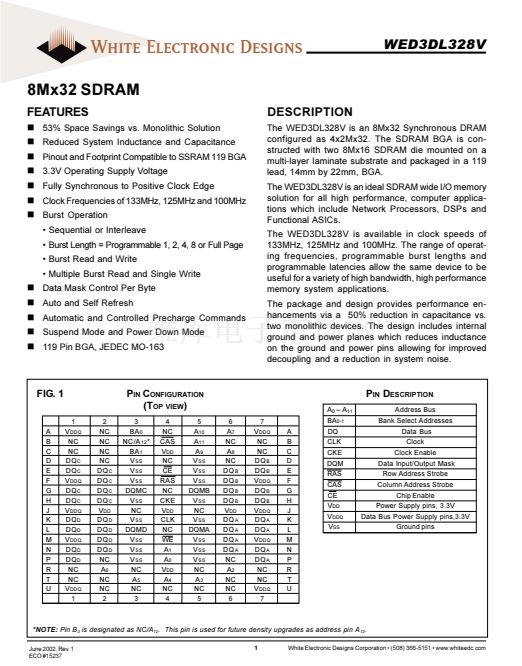
FIG. 1
1
V
DDQ
NC
NC
DQ
C
DQ
C
V
DDQ
DQ
C
DQ
C
V
DDQ
DQ
D
DQ
D
V
DDQ
DQ
D
DQ
D
NC
NC
V
DDQ
1
2
NC
NC
NC
NC
DQ
C
DQ
C
DQ
C
DQ
C
V
DD
DQ
D
DQ
D
DQ
D
DQ
D
NC
A
6
NC
NC
2
P
IN
C
ONFIGURATION
(T
OP VIEW
)
3
BA
0
NC/A
12
*
BA
1
V
SS
V
SS
V
SS
DQMC
V
SS
NC
V
SS
DQMD
V
SS
V
SS
V
SS
NC
A
5
NC
3
4
NC
CAS
V
DD
NC
CE
RAS
NC
CKE
V
DD
CLK
NC
WE
A
1
A
0
V
DD
A
4
NC
4
5
A
10
A
11
A
9
V
SS
V
SS
V
SS
DQMB
V
SS
NC
V
SS
DQMA
V
SS
V
SS
V
SS
NC
A
3
NC
5
6
A
7
NC
A
8
NC
DQ
B
DQ
B
DQ
B
DQ
B
V
DD
DQ
A
DQ
A
DQ
A
DQ
A
NC
A
2
NC
NC
6
7
V
DDQ
NC
NC
DQ
B
DQ
B
V
DDQ
DQ
B
DQ
B
V
DDQ
DQ
A
DQ
A
V
DDQ
DQ
A
DQ
A
NC
NC
V
DDQ
7
A
B
C
D
E
F
G
H
J
K
L
M
N
P
R
T
U
P
IN
D
ESCRIPTION
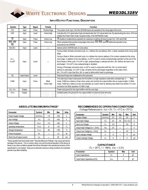
A
0
聳 A
11
BA
0-1
DQ
CLK
CKE
DQM
RAS
CAS
CE
V
DD
V
DDQ
V
SS
Address Bus
Bank Select Addresses
Data Bus
Clock
Clock Enable
Data Input/Output Mask
Row Address Strobe
Column Address Strobe
Chip Enable
Power Supply pins, 3.3V
Data Bus Power Supply pins,3.3V
Ground pins
A
B
C
D
E
F
G
H
J
K
L
M
N
P
R
T
U
*NOTE:
Pin B
3
is designated as NC/A
12
. This pin is used for future density upgrades as address pin A
12
.
June 2002, Rev. 1
ECO #15237
1
White Electronic Designs Corporation 聲 (508) 366-5151 聲 www.whiteedc.com


 1
1
 2
2
 3
3
 4
4
 5
5
 6
6
 7
7
 8
8
 9
9
 10
10
 11
11
 12
12
 13
13
 14
14
 15
15
 16
16
 17
17
 18
18
 19
19
 20
20
 21
21
 22
22
 23
23
 24
24
 25
25
 26
26
 27
27
