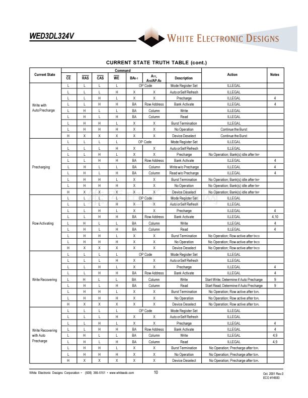
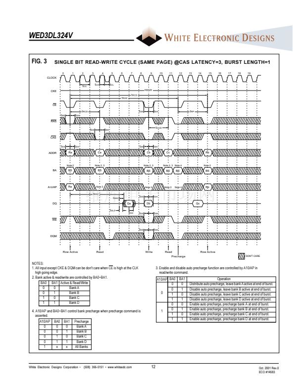
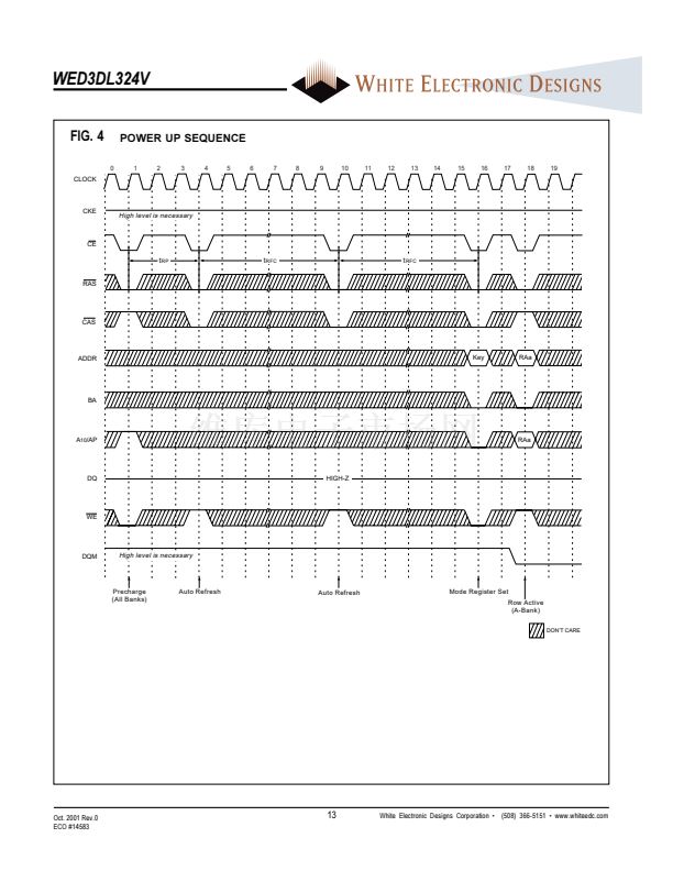
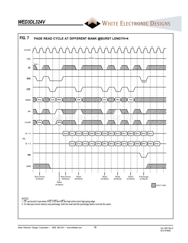
WED3DL324V
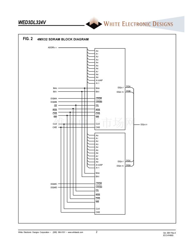
4Mx32 SDRAM
FEATURES
n
53% Space Savings vs. Monolithic Solution
n
Reduced System Inductance and Capacitance
n
Pinout and Footprint Compatible to SSRAM 119 BGA
n
3.3V Operating Supply Voltage
n
Fully Synchronous to Positive Clock Edge
n
Clock Frequencies of 133, 125 and 100MHz
n
Burst Operation
聲 Sequential or Interleave
聲 Burst Length = Programmable 1, 2, 4, 8 or Full Page
聲 Burst Read and Write
聲 Multiple Burst Read and Single Write
n
Data Mask Control Per Byte
n
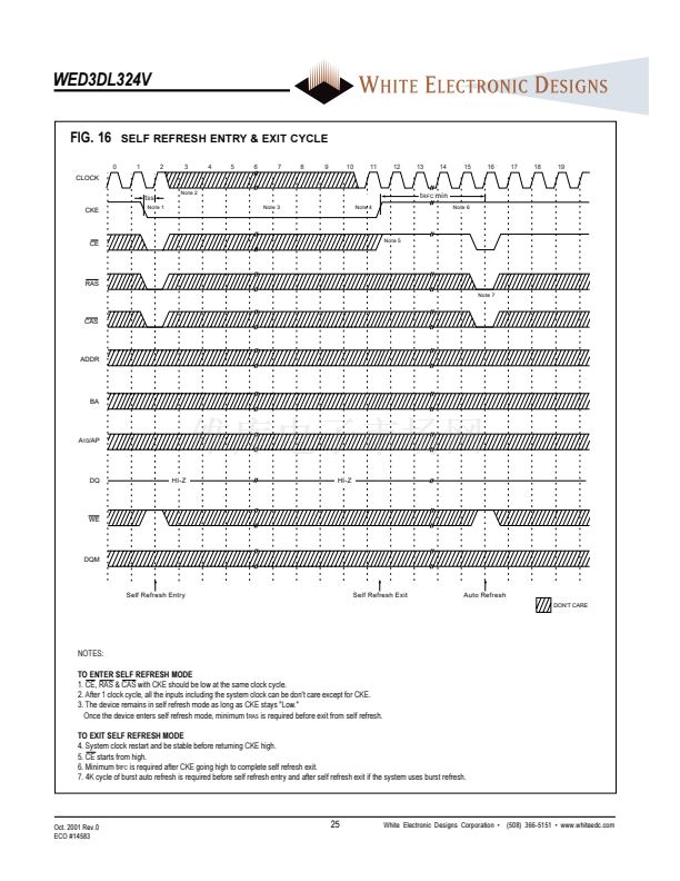
Auto and Self Refresh
n
Automatic and Controlled Precharge Commands
n
Suspend Mode and Power Down Mode
n
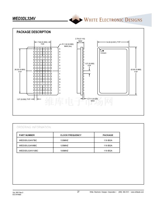
119 Pin BGA, JEDEC MO-163
DESCRIPTION
The WED3DL324V is a 4Mx32 Synchronous DRAM configured
as 4x1Mx32. The SDRAM BGA is constructed with two 4Mx16
SDRAM die mounted on a multi-layer laminate substrate and
packaged in a 119 lead, 14mm by 22mm, BGA.
The WED3DL324V is available in clock speeds of 133MHz,
125MHz and 100MHz. The range of operating frequencies, pro-
grammable burst lengths and programmable latencies allow the
same device to be useful for a variety of high bandwidth, high
performance memory system applications.
The package and design provides performance enhancements
via a 50% reduction in capacitance vs. two monolithic devices.
The design includes internal ground and power planes which
reduces inductance on the ground and power pins allowing for
improved decoupling and a reduction in system noise.
FIG. 1
A
B
C
D
E
F
G
H
J
K
L
M
N
P
R
T
U
PINOUT (TOP VIEW)
1
VDDQ
NC
NC
DQC
DQC
VDDQ
DQC
DQC
VDDQ
DQD
DQD
VDDQ
DQD
DQD
NC
NC
VDDQ
1
2
NC
NC
NC
NC
DQC
DQC
DQC
DQC
VDD
DQD
DQD
DQD
DQD
NC
A6
NC
NC
2
3
BA0
NC/A12*
BA1
VSS
VSS
VSS
DQMC
VSS
NC
VSS
DQMD
VSS
VSS
VSS
NC
A5
NC
3
4
NC
CAS
VDD
NC
CE
RAS
NC
CKE
VDD
CLK
NC
WE
A1
A0
VDD
A4
NC
4
5
A10
A11
A9
VSS
VSS
VSS
DQMB
VSS
NC
VSS
DQMA
VSS
VSS
VSS
NC
A3
NC
5
6
A7
NC
A8
NC
DQB
DQB
DQB
DQB
VDD
DQA
DQA
DQA
DQA
NC
A2
NC
NC
6
7
VDDQ
NC
NC
DQB
DQB
VDDQ
DQB
DQB
VDDQ
DQA
DQA
VDDQ
DQA
DQA
NC
NC
VDDQ
7
A
B
C
D
E
F
G
H
J
K
L
M
N
P
R
T
U
BA0-1
DQ
CLK
CKE
DQM
RAS
CAS
CE
VDD
VDDQ
VSS
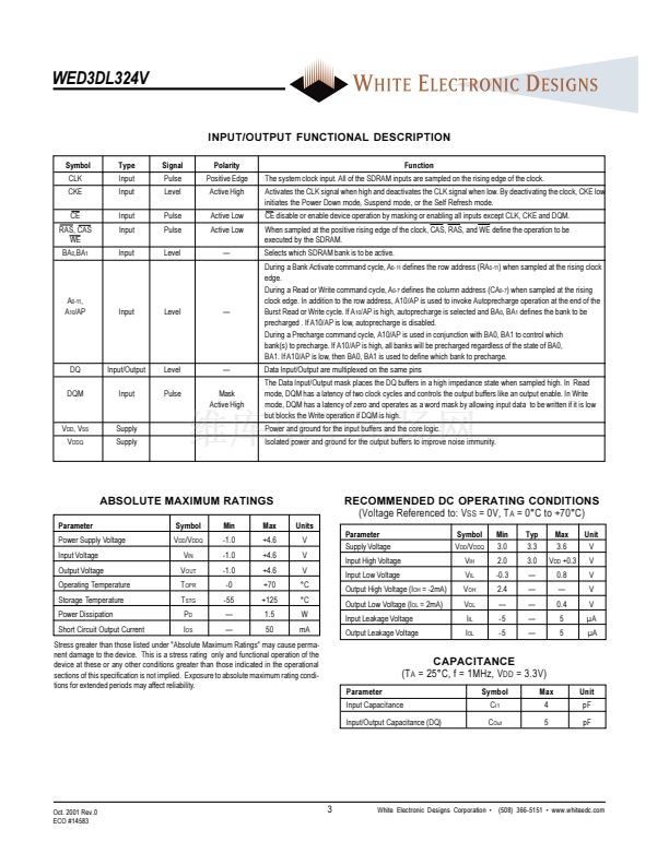
PIN DESCRIPTION
A0 聳 A11
Address Bus
Bank Select Addresses
Data Bus
Clock
Clock Enable
Data Input/Output Mask
Row Address Strobe
Column Address Strobe
Chip Enable
Power Supply pins, 3.3V
Data Bus Power Supply pins,3.3V
Ground pins
*NOTE:
Pin B3 is designated as NC/A12. This pin is used for future density upgrades as address pin A12.
Oct. 2001 Rev.0
ECO #14583
1
White Electronic Designs Corporation 聲 (508) 366-5151 聲 www.whiteedc.com


 1
1
 2
2
 3
3
 4
4
 5
5
 6
6
 7
7
 8
8
 9
9
 10
10
 11
11
 12
12
 13
13
 14
14
 15
15
 16
16
 17
17
 18
18
 19
19
 20
20
 21
21
 22
22
 23
23
 24
24
 25
25
 26
26
 27
27
