1WCFS0808V1E
WCFS0808V1E
32K x 8 3.3V Static RAM
Features
鈥?Single 3.3V power supply
鈥?Ideal for low-voltage cache memory applications
鈥?High speed
鈥?12/15 ns
鈥?Plastic SOJ and TSOP packaging
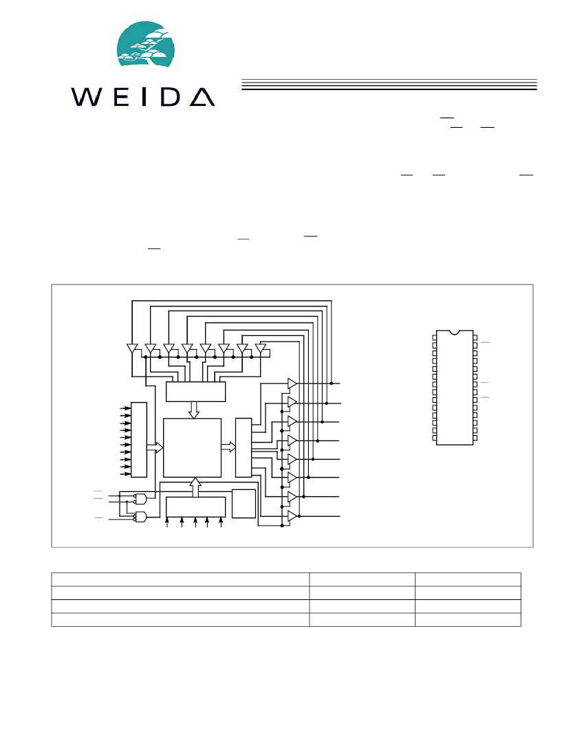
An active LOW Write Enable signal (WE) controls the writing/
reading operation of the memory. When CE and WE inputs are
both LOW, data on the eight data input/output pins (I/O
0
through I/O
7
) is written into the memory location addressed by
the address present on the address pins (A
0
through A
14
).
Reading the device is accomplished by selecting the device
and enabling the outputs, CE and OE active LOW, while WE
remains inactive or HIGH. Under these conditions, the con-
tents of the location addressed by the information on address
pins is present on the eight data input/output pins.
The input/output pins remain in a high-impedance state unless
the chip is selected, outputs are enabled, and Write Enable
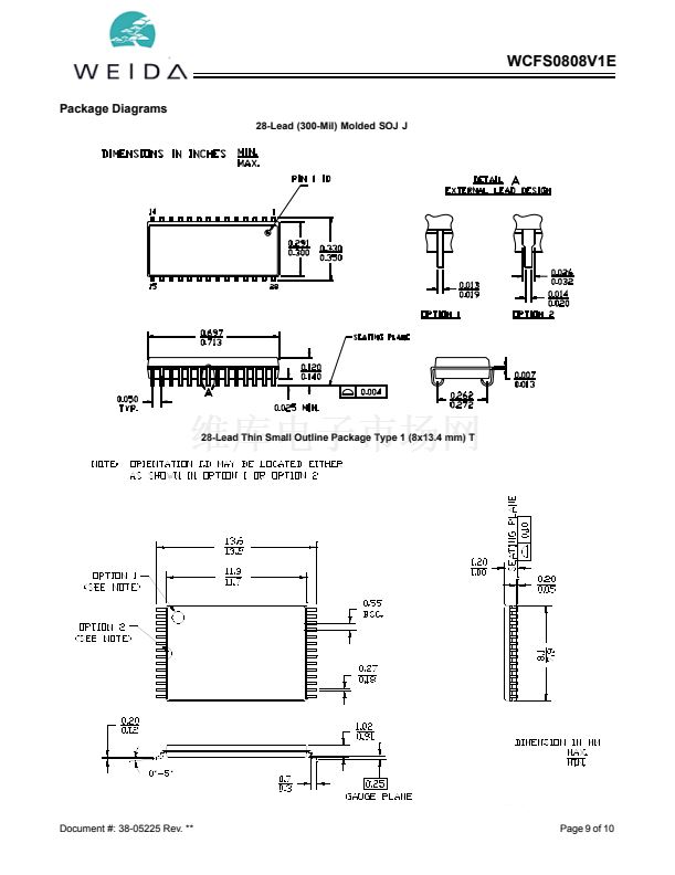
(WE) is HIGH. The WCFS0808V1E is available in 28-pin stan-
dard 300-mil-wide SOJ and TSOP Type I packages.
Functional Description
The WCFS0808V1E is a high-performance 3.3V CMOS Static
RAM organized as 32K words by 8 bits. Easy memory expan-
sion is provided by an active LOW Chip Enable (CE) and ac-
tive LOW Output Enable (OE) and three-state drivers. The de-
vice has an automatic power-down feature, reducing the
power consumption by more than 95% when deselected.
Logic Block Diagram
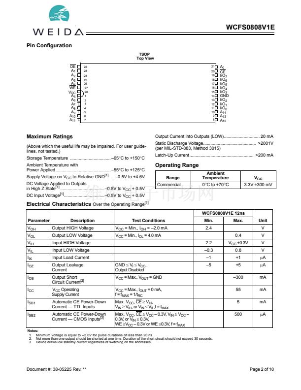
Pin Configurations
SOJ
Top View
A
5
A
6
A
7
A
8
A
9
A
10
A
11
A
12
A
13
A
14
I/O
0
I/O
1
I/O
2
GND
1
2
3
4
5
6
7
8
9
10
11
12
13
14
28
27
26
25
24
23
22
21
20
19
18
17
16
15
V
CC
WE
A
4
A
3
A
2
A
1
OE
A
0
CE
I/O
7
I/O
6
I/O
5
I/O
4
I/O
3
INPUT BUFFER
I/O
0
I/O
1
A
0
A
1
A
2
A
3
A
4
A
5
A
6
A
7
A
8
A
9
CE
WE
OE
ROW DECODER
I/O
2
SENSE AMPS
32K x 8
ARRAY
I/O
3
I/O
4
I/O
5
COLUMN
DECODER
POWER
DOWN
I/O
6
I/O
7
A
10
A
11
A
12
A
13
Selection Guide
WCFS0808V1E 12ns
Maximum Access Time (ns)
Maximum Operating Current (mA)
Maximum CMOS Standby Current (碌A)
12
55
500
WCFS0808V1E 15ns
15
50
500
Document #: 38-05225 Rev. **
A
14
Revised February 11, 2002


 1
1
 2
2
 3
3
 4
4
 5
5
 6
6
 7
7
 8
8
 9
9
 10
10
