W986432DH
512K
脳
4 BANKS
脳
32 BITS SDRAM
Table of Contents-
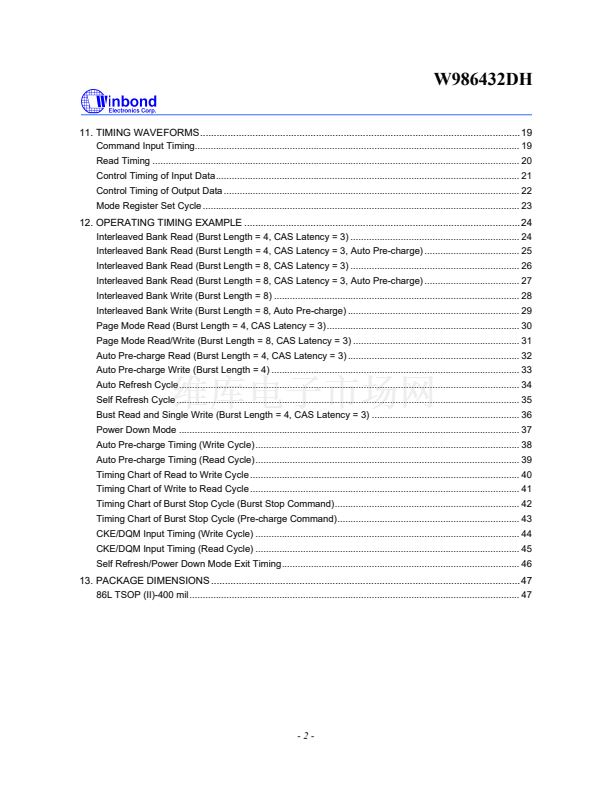
1. GENERAL DESCRIPTION ..................................................................................................................3
2. FEATURES ..........................................................................................................................................3
3. AVAILABLE PART NUMBER...............................................................................................................3
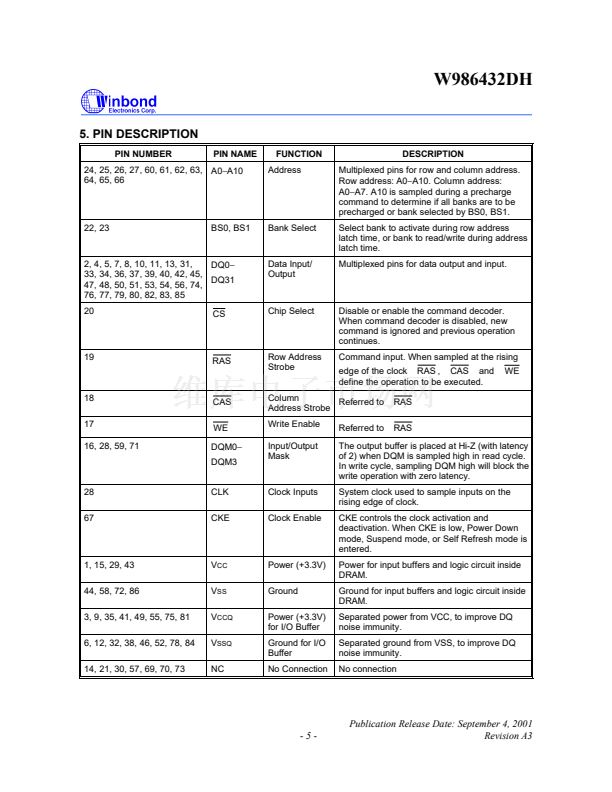
4. PIN CONFIGURATION........................................................................................................................4
5. PIN DESCRIPTION..............................................................................................................................5
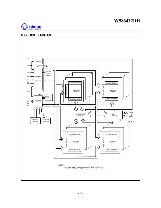
6. BLOCK DIAGRAM ...............................................................................................................................6
7. FUNCTIONAL DESCRIPTION ............................................................................................................7
Power Up and Initialization ....................................................................................................................... 7
Programming Mode Register .................................................................................................................... 7
Bank Activate Command .......................................................................................................................... 7
Read and Write Access Modes ................................................................................................................ 7
Burst Read Command .............................................................................................................................. 8
Burst Command ........................................................................................................................................ 8
Read Interrupted by a Read ..................................................................................................................... 8
Read Interrupted by a Write ..................................................................................................................... 8
Write Interrupted by a Write ..................................................................................................................... 8
Write Interrupted by a Read ..................................................................................................................... 8
Burst Stop Command ............................................................................................................................... 8
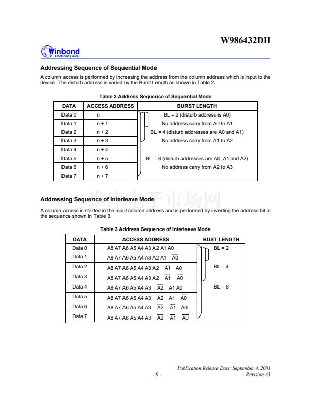
Addressing Sequence of Sequential Mode .............................................................................................. 9
Addressing Sequence of Interleave Mode................................................................................................ 9
Auto Pre-charge Command .................................................................................................................... 10
Precharge Command.............................................................................................................................. 10
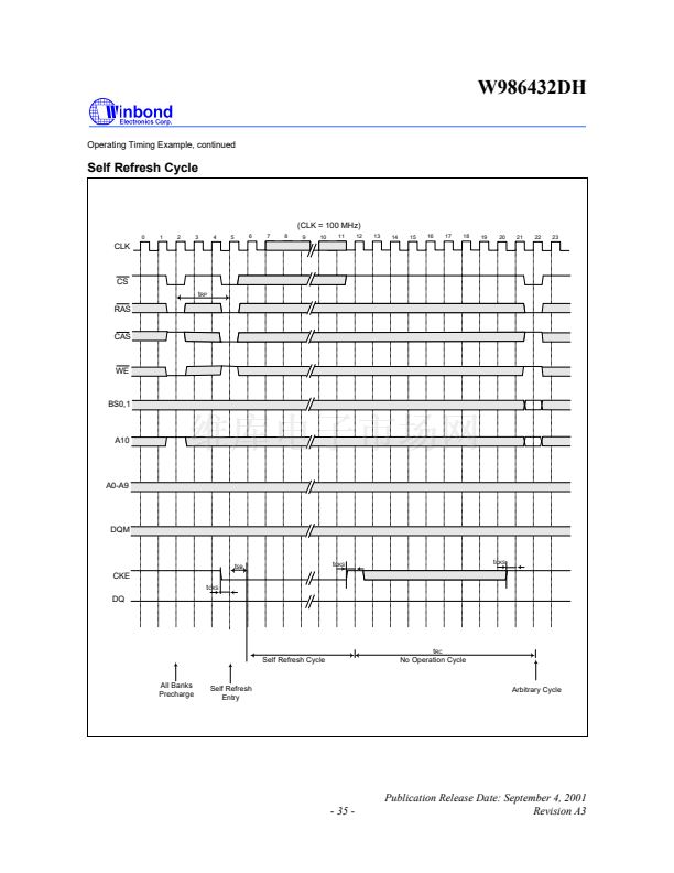
Self Refresh Command .......................................................................................................................... 10
Power Down Mode ................................................................................................................................. 10
No Operation Command ......................................................................................................................... 11
Deselect Command ................................................................................................................................ 11
Clock Suspend Mode.............................................................................................................................. 11
8. TABLE OF OPERATING MODES .....................................................................................................12
9. SIMPLIFIED STATE DIAGRAM.........................................................................................................13
10. ELECTRICAL CHARACTERISTICS................................................................................................14
Absolute Maximum Rating...................................................................................................................... 14
Recommended DC Operating Conditions .............................................................................................. 14
Capacitance............................................................................................................................................ 14
DC Characteristics.................................................................................................................................. 15
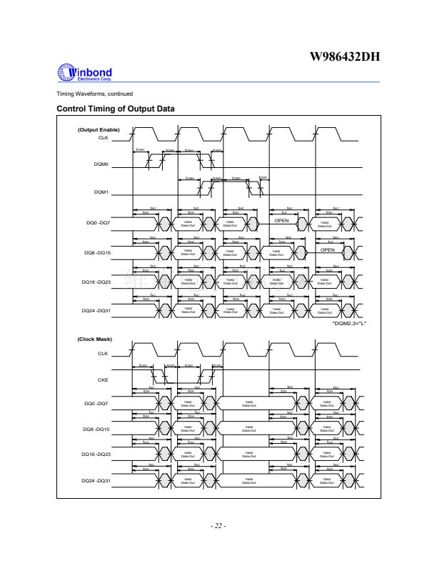
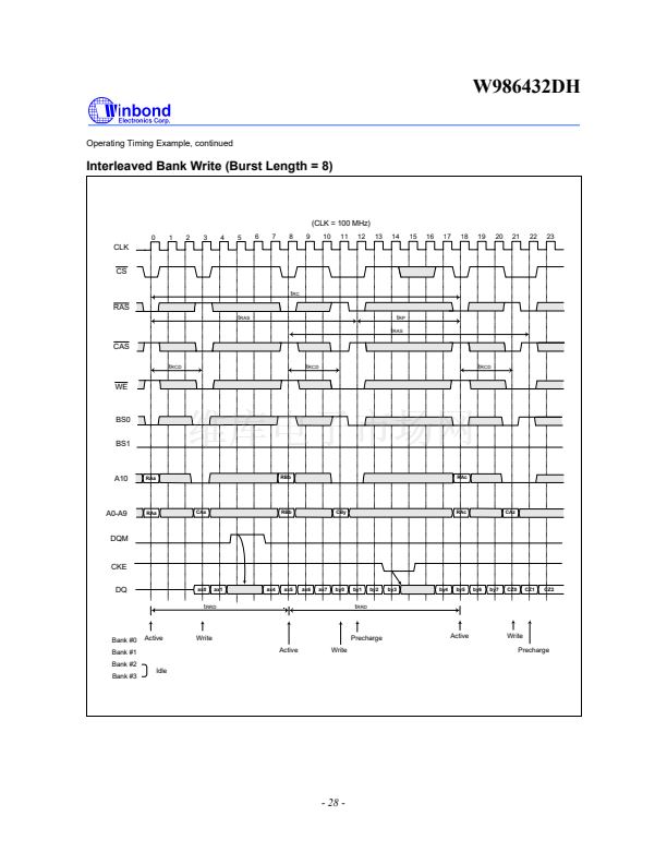
AC Characteristics .................................................................................................................................. 16
Publication Release Date: September 4, 2001
Revision A3
-1-


 1
1
 2
2
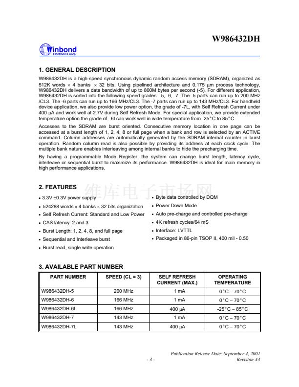 3
3
 4
4
 5
5
 6
6
 7
7
 8
8
 9
9
 10
10
 11
11
 12
12
 13
13
 14
14
 15
15
 16
16
 17
17
 18
18
 19
19
 20
20
 21
21
 22
22
 23
23
 24
24
 25
25
 26
26
 27
27
 28
28
 29
29
 30
30
 31
31
 32
32
 33
33
 34
34
 35
35
 36
36
 37
37
 38
38
 39
39
 40
40
 41
41
 42
42
 43
43
 44
44
 45
45
 46
46
 47
47
 48
48
