W134M/W134S
Direct Rambus鈩?Clock Generator
Features
鈥?Differential clock source for Direct Rambus鈩?memory
subsystem for up to 800-MHz data transfer rate
鈥?Provide synchronization flexibility: the Rambus
廬
Chan-
nel can optionally be synchronous to an external sys-
tem or processor clock
鈥?Power managed output allows Rambus Channel clock
to be turned off to minimize power consumption for
mobile applications
鈥?Works with Cypress CY2210, W133, W158, W159, W161,
and W167 to support Intel
廬
architecture platforms
鈥?Low-power CMOS design packaged in a 24-pin, 150-mil
SSOP package
Overview
The Cypress W134M/W134S provides the differential clock
signals for a Direct Rambus memory subsystem. It includes
signals to synchronize the Direct Rambus Channel clock to an
external system clock but can also be used in systems that do
not require synchronization of the Rambus clock.
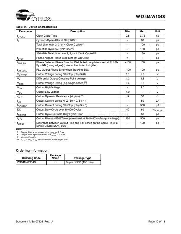
Key Specifications
Supply Voltage: ..................................... V
DD
= 3.3V鹵0.165V
Operating Temperature: .................................. 0擄C to +70擄C
Input Threshold: .................................................. 1.5V typical
Maximum Input Voltage:.........................................V
DD
+0.5V
Maximum Input Frequency: ..................................... 100 MHz
Output Duty Cycle: .................................. 40/60% worst case
Output Type:........................... Rambus signaling level (RSL)
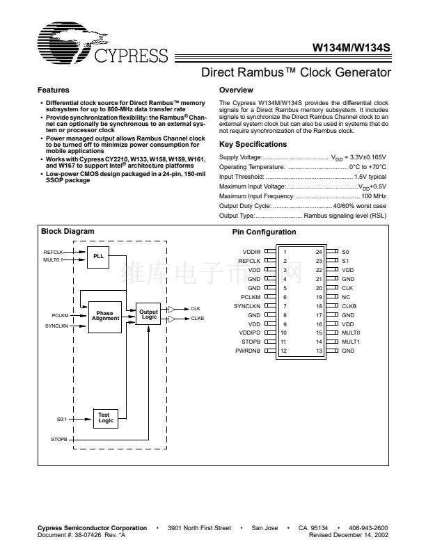
Block Diagram
REFCLK
MULT0:1
Pin Configuration
VDDIR
REFCLK
VDD
GND
GND
PCLKM
SYNCLKN
GND
VDD
VDDIPD
STOPB
PWRDNB
1
2
3
4
5
6
7
8
9
10
11
12
24
23
22
21
20
19
18
17
16
15
14
13
S0
S1
VDD
GND
CLK
NC
CLKB
GND
VDD
MULT0
MULT1
GND
PLL
PCLKM
SYNCLKN
Phase
Alignment
Output
Logic
CLK
CLKB
S0:1
Test
Logic
STOPB
Cypress Semiconductor Corporation
Document #: 38-07426 Rev. *A
鈥?/div>
3901 North First Street
鈥?/div>
San Jose
鈥?/div>
CA 95134 鈥?408-943-2600
Revised December 14, 2002


 1
1
 2
2
 3
3
 4
4
 5
5
 6
6
 7
7
 8
8
 9
9
 10
10
 11
11
 12
12
 13
13
