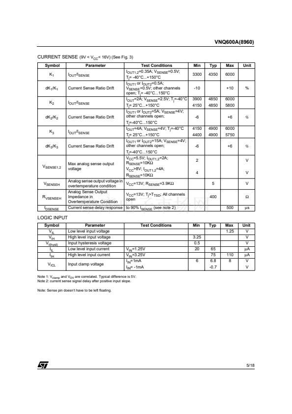
30m鈩?/div>
I
lim
25A
V
CC
36 V
(*) Per each channel at V
CC
=13V
DC SHORT CIRCUIT CURRENT: 25A
s
CMOS COMPATIBLE INPUTS
s
PROPORTIONAL LOAD CURRENT SENSE
s
UNDERVOLTAGE & OVERVOLTAGE
n
SHUT-DOWN
s
OVERVOLTAGE CLAMP
s
THERMAL SHUT-DOWN
s
CURRENT LIMITATION
s
VERY LOW STAND-BY POWER DISSIPATION
s
PROTECTION AGAINST:
n
LOSS OF GROUND & LOSS OF V
CC
s
REVERSE BATTERY PROTECTION (**)
s
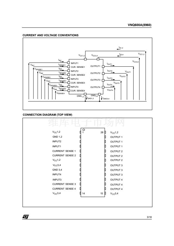
SO-28 (DOUBLE ISLAND)
ORDER CODES
PACKAGE
TUBE
T&R
SO-28
VNQ600A(8960) VNQ600A(8960)TR
DESCRIPTION
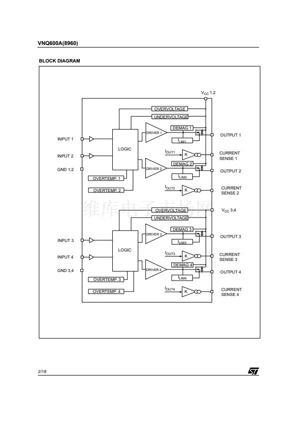
The VNQ600A(8960) is a quad HSD formed by
assembling two VND600 chips in the same SO-28
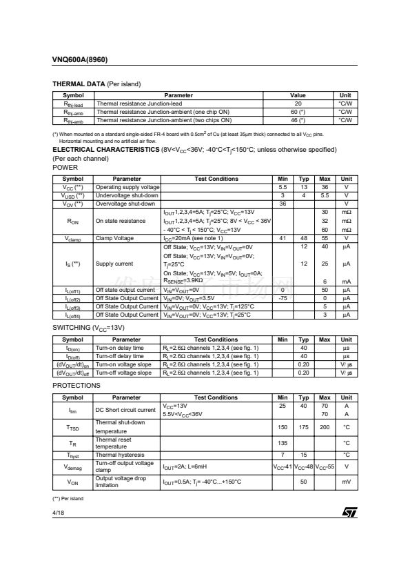
ABSOLUTE MAXIMUM RATING
Symbol
V
CC
-V
CC
I
OUT
I
R
I
IN
V
CSENSE
I
GND
Parameter
package. The VND600 is a monolithic device
designed in| STMicroelectronics VIPower M0-3
Technology. The VNQ600A(8960) is intended for
driving any type of multiple loads with one side
connected to ground. This device has four
independent channels and four analog sense
outputs which deliver currents proportional to the
outputs currents. Active current limitation
combined with thermal shut-down and automatic
restart protect the device against overload. Device
automatically turns off in case of ground pin
disconnection.
Value
41
-0.3
15
-15
+/- 10
-3
+15
-200
4000
2000
5000
5000
126
6.25
Internally Limited
-55 to 150
Unit
V
V
A
A
mA
V
V
mA
V
V
V
V
mJ
W
擄C
擄C
Supply voltage (continuous)
Reverse supply voltage (continuous)
Output current (continuous), for each channel
Reverse output current (continuous), for each channel
Input current
Current sense maximum voltage
Ground current at T
pins
< 25擄C (continuous)
Electrostatic Discharge (Human Body Model: R=1.5K鈩? C=100pF)
- INPUT
- CURRENT SENSE
- OUTPUT
- V
CC
Maximum Switching Energy
(L=0.11mH; R
L
=0鈩? V
bat
=13.5V; T
jstart
=150潞C; I
L
=40A)
Power dissipation (per island) at T
lead
=25擄C
Junction operating temperature
Storage temperature
V
ESD
E
MAX
P
tot
T
j
T
stg
(**) See application schematic at page 9.
June 2003
1/18


 1
1
 2
2
 3
3
 4
4
 5
5
 6
6
 7
7
 8
8
 9
9
 10
10
 11
11
 12
12
 13
13
 14
14
 15
15
 16
16
 17
17
 18
18
