VIS
Description
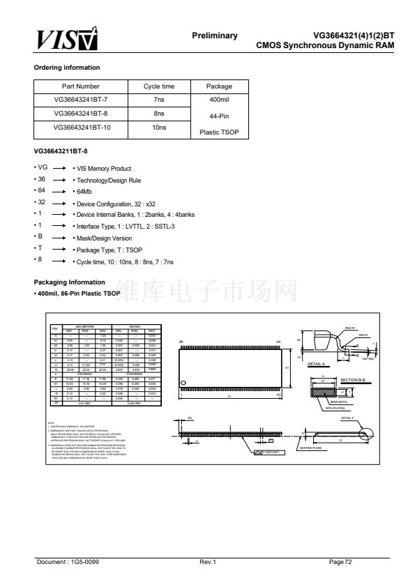
Preliminary
VG3664321(4)1(2)BT
CMOS Synchronous Dynamic RAM
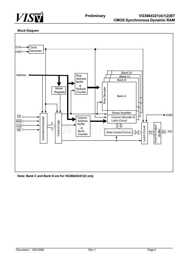
The device is CMOS Synchronous Dynamic RAM organized as 524,288 - word x 32 - bit x 4 -
bank, and 1,048,576 - word x 32 - bit x 2 - bank, respectively. lt is fabricated with an advanced
submicron CMOS technology and designed to operate from a singly 3.3V only power supply. It is
packaged in JEDEC standard pinout and standard plastic TSOP package.
Features
鈥?Single 3.3V (
鹵
0.3V ) power supply
鈥?High speed clock cycle time : 8/10 for LVTTL
鈥?High speed clock cycle time : 8/10 for SSTL - 3
鈥?Fully synchronous with all signals referenced to a positive clock edge
鈥?Programmable CAS Iatency (2,3)
鈥?Programmable burst length (1,2,4,8,& Full page)
鈥?Programmable wrap sequence (Sequential/Interleave)
鈥?Automatic precharge and controlled precharge
鈥?Auto refresh and self refresh modes
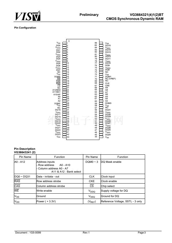
鈥?Dual Internal banks controlled by A11 (Bank select) for VG36643211(2)
鈥?Quad Internal banks controlled by A11 & A12 (Bank select) for VG36643241(2)
鈥?Each Banks can operate simultaneously and independently
鈥?LVTTL compatible I/O interface for VG36643211 and VG36643241
鈥?SSTL - 3 compatible I/O interface for VG36643212 and VG36643242
鈥?Random column access in every cycle
鈥?x32 organization
鈥?Input/Output controlled by DQM0 ~ 3
鈥?4,096 refresh cycles/64ms
鈥?Burst termination by burst stop and precharge command
鈥?Burst read/single write option
Document : 1G5-0099
Rev.1
Page 1


 1
1
 2
2
 3
3
 4
4
 5
5
 6
6
 7
7
 8
8
 9
9
 10
10
 11
11
 12
12
 13
13
 14
14
 15
15
 16
16
 17
17
 18
18
 19
19
 20
20
 21
21
 22
22
 23
23
 24
24
 25
25
 26
26
 27
27
 28
28
 29
29
 30
30
 31
31
 32
32
 33
33
 34
34
 35
35
 36
36
 37
37
 38
38
 39
39
 40
40
 41
41
 42
42
 43
43
 44
44
 45
45
 46
46
 47
47
 48
48
 49
49
 50
50
 51
51
 52
52
 53
53
 54
54
 55
55
 56
56
 57
57
 58
58
 59
59
 60
60
 61
61
 62
62
 63
63
 64
64
 65
65
 66
66
 67
67
 68
68
 69
69
 70
70
 71
71
 72
72
