鈻?/div>
QFC options for FET control. x4 parts.
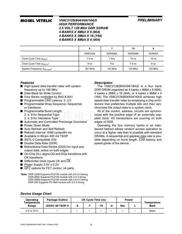
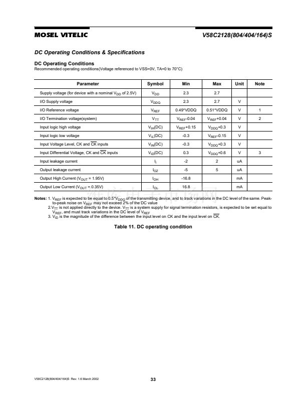
*Note: DDR 333B Supports PC2700 module with 2.5-3-3 timing
DDR 266A Supports PC2100 module with 2-3-3 timing
DDR 266B Supports PC2100 module with 2.5-3-3 timing
DDR 200 Supports PC1600 module with 2-2-2 timing
CILETIV LESO M
8
DDR200
10 ns
8 ns
125 MHz
DDR266B
10 ns
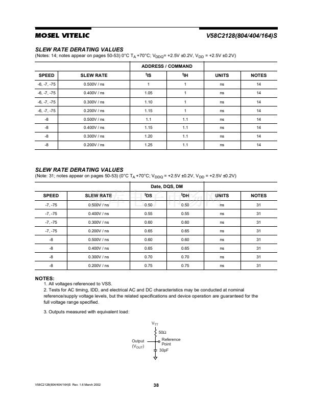
7.5 ns
133 MHz
Clock Cycle Time (t
CK2
)
Clock Cycle Time (t
CK2.5
)
System Frequency (f
CK max
)
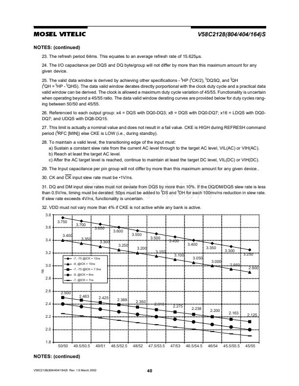
7.5 ns
6 ns
167 MHz
Description
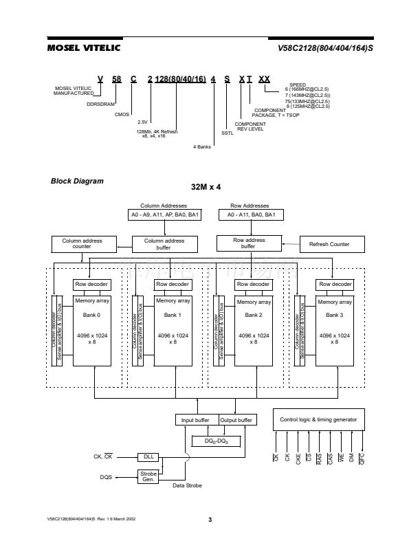
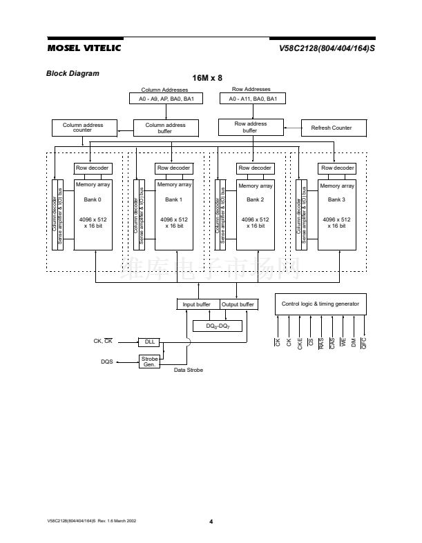
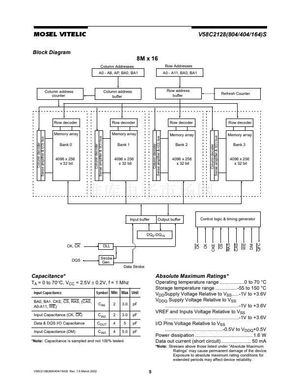
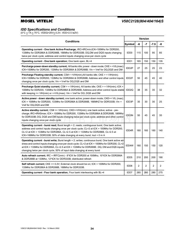
The V58C2128(804/404/164)S is a four bank
DDR DRAM organized as 4 banks x 4Mbit x 8 (804),
4 banks x 2Mbit x 16 (404), or 4 banks x 8Mbit x 4
(164). The V58C2128(804/404/164)S achieves high
speed data transfer rates by employing a chip archi-
tecture that prefetches multiple bits and then syn-
chronizes the output data to a system clock.
All of the control, address, circuits are synchro-
nized with the positive edge of an externally sup-
plied clock. I/O transactions are ocurring on both
edges of DQS.
Operating the four memory banks in an inter-
leaved fashion allows random access operation to
occur at a higher rate than is possible with standard
DRAMs. A sequential and gapless data rate is pos-
sible depending on burst length, CAS latency and
speed grade of the device.
Device Usage Chart
Operating
Temperature
Range
0擄C to 70擄C
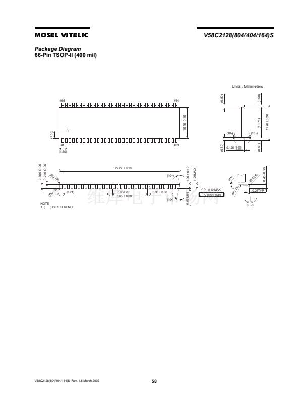
Package Outline
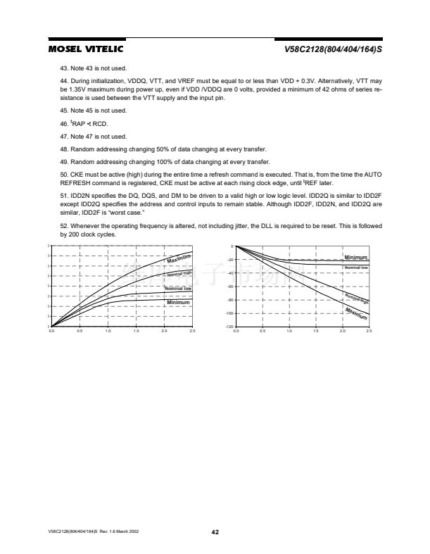
JEDEC 66 TSOP II
鈥?/div>
CK Cycle Time (ns)
-6
鈥?/div>
Power
-8
鈥?/div>
-7
鈥?/div>
-75
鈥?/div>
Std.
鈥?/div>
L
鈥?/div>
Temperature
Mark
Blank
V58C2128(804/404/164)S Rev.1.6 March 2002
1
V58C2128804S相關(guān)型號PDF文件下載
-
型號
版本
描述
廠商
下載
-
英文版
HIGH PERFORMANCE 2.5 VOLT 128 Mbit DDR SDRAM
MOSEL
-
英文版
HIGH PERFORMANCE 2.5 VOLT 128 Mbit DDR SDRAM
MOSEL [Mos...
-
英文版
HIGH PERFORMANCE 2.5 VOLT 256 Mbit DDR SDRAM
MOSEL [Mos...
-
英文版
64 Mbit DDR SDRAM 2.5 VOLT 4M X 16
MOSEL
-
英文版
64 Mbit DDR SDRAM 2.5 VOLT 4M X 16
MOSEL [Mos...
-
英文版
HIGH PERFORMANCE 2.5 VOLT 16M X 4 DDR SDRAM 4 BANKS X 4Mbit ...
MOSEL
-
英文版
HIGH PERFORMANCE 2.5 VOLT 16M X 4 DDR SDRAM 4 BANKS X 4Mbit ...
MOSEL [Mos...
-
英文版
HIGH PERFORMANCE 2.5 VOLT 8M X 8 DDR SDRAM 4 BANKS X 2Mbit X...
MOSEL
-
英文版
HIGH PERFORMANCE 2.5 VOLT 8M X 8 DDR SDRAM 4 BANKS X 2Mbit X...
MOSEL [Mos...
-
英文版
64 Mbit DDR SDRAM 4M X 16, 3.3VOLT
MOSEL
-
英文版
64 Mbit DDR SDRAM 4M X 16, 3.3VOLT
MOSEL [Mos...
-
英文版
HIGH PERFORMANCE 2.5 VOLT 128 Mbit DDR SDRAM
MOSEL
-
英文版
HIGH PERFORMANCE 2.5 VOLT 128 Mbit DDR SDRAM
MOSEL [Mos...
-
英文版
HIGH PERFORMANCE 2.5 VOLT 128 Mbit DDR SDRAM
MOSEL
-
英文版
HIGH PERFORMANCE 2.5 VOLT 128 Mbit DDR SDRAM
MOSEL [Mos...
-
英文版
HIGH PERFORMANCE 2.5 VOLT 128 Mbit DDR SDRAM
MOSEL
-
英文版
HIGH PERFORMANCE 2.5 VOLT 128 Mbit DDR SDRAM
MOSEL [Mos...
-
英文版
HIGH PERFORMANCE 2.5 VOLT 256 Mbit DDR SDRAM
MOSEL [Mos...
-
英文版
HIGH PERFORMANCE 2.5 VOLT 256 Mbit DDR SDRAM
MOSEL [Mos...
-
英文版
HIGH PERFORMANCE 2.5 VOLT 256 Mbit DDR SDRAM
MOSEL [Mos...


 1
1
 2
2
 3
3
 4
4
 5
5
 6
6
 7
7
 8
8
 9
9
 10
10
 11
11
 12
12
 13
13
 14
14
 15
15
 16
16
 17
17
 18
18
 19
19
 20
20
 21
21
 22
22
 23
23
 24
24
 25
25
 26
26
 27
27
 28
28
 29
29
 30
30
 31
31
 32
32
 33
33
 34
34
 35
35
 36
36
 37
37
 38
38
 39
39
 40
40
 41
41
 42
42
 43
43
 44
44
 45
45
 46
46
 47
47
 48
48
 49
49
 50
50
 51
51
 52
52
 53
53
 54
54
 55
55
 56
56
 57
57
 58
58
 59
59
