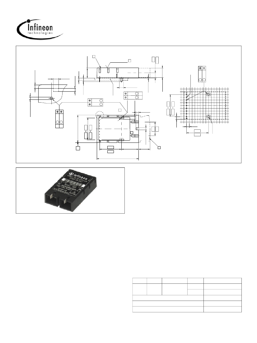
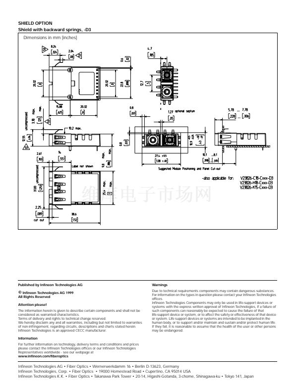
鈭?/div>
0.3 M
(25.25鹵0.05)
.994鹵.002
A
A
1 2 3 4 5
8x
.1
.8
8x
2.54
20.32
6 7 8 9
20.32
.8
20.32
(2.5鹵0.1)
.098鹵.002
1
DUPLEX
SC 5
RECEPTACLE
.8
(2.54)
.1
(2.54)
.1
20.32
.8
(1.9鹵0.1) 2x
.075鹵.004
12.7
.5
(2.05鹵0.05)
.079鹵.002
(38.6鹵0.15)
1.52鹵.006
32
(15.88鹵0.5)
.625鹵.02
3
(11 max)
.433 max
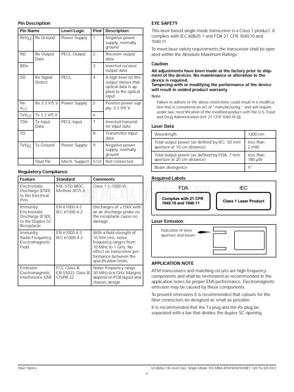
Absolute Maximum Ratings
Exceeding any one of these values may destroy the device
immediately.
Package Power Dissipation
(1) ........................................................
1.5 W
Supply Voltage (V
CC
鈥揤
EE
) 5 V............................................. 7 V
3.3 V.......................................... 5 V
Data Input Levels........................................................V
CC
+0.5 V
Differential Data Input Voltage ............................................ 2.5 V
Operating Ambient Temperature .............................0擄C to 70擄C
Storage Ambient Temperature ............................ 鈥?0擄C to 85擄C
Soldering Conditions Temp/Time
(MIL
-STD 883C, Method 2003) ............................. 250擄C/5.5s
Note
1. For V
CC
鈥揤
EE
(min., max.). 50% duty cycle. The supply current does
not include the load drive current of the receiver output.
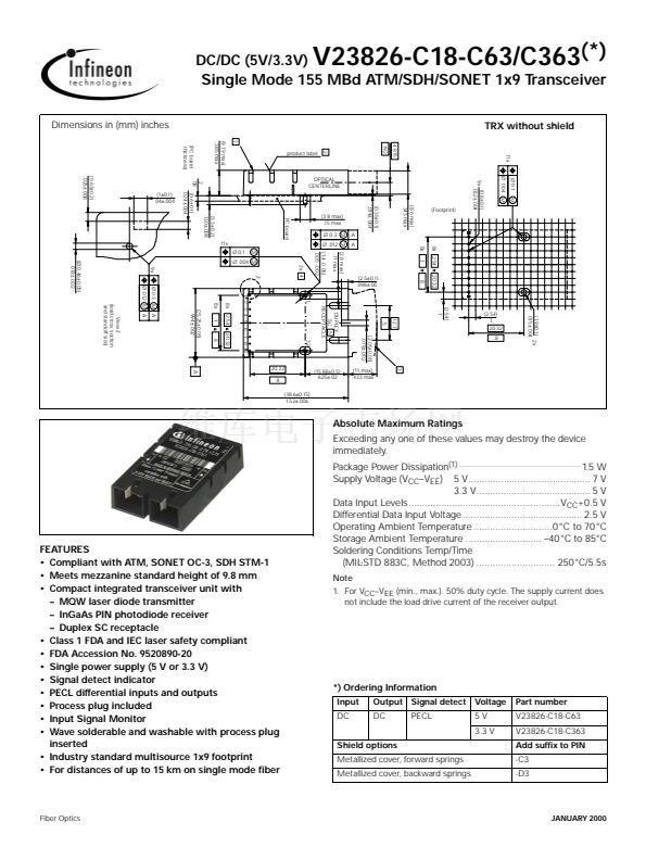
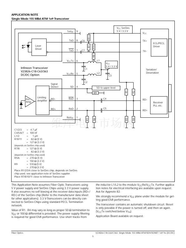
*) Ordering Information
Input
DC
Output Signal detect
DC
PECL
Voltage
5V
3.3 V
Shield options
Metallized cover, forward springs
Metallized cover, backward springs
Part number
V23826-C18-C63
V23826-C18-C363
Add suffix to PIN
-C3
-D3
JANUARY 2000


 1
1
 2
2
 3
3
 4
4
 5
5
 6
6
 7
7
 8
8
