Standard Products
QCOTS
TM
UT8Q512 512K x 8 SRAM
Data Sheet
April, 2002
FEATURES
q
25ns (3.3 volt supply) maximum address access time
q
Asynchronous operation for compatibility with industry-
standard 512K x 8 SRAMs
TTL compatible inputs and output levels, three-state
bidirectional data bus
q
Typical radiation performance
- Total dose: 50krads
- >100krads(Si), for any orbit, using Aeroflex UTMC
patented shielded package
- SEL Immune >80 MeV-cm
2
/mg
- LET
TH
(0.25) = >10 MeV-cm
2
/mg
- Saturated Cross Section cm
2
per bit, 5.0E-9
- <1E-8 errors/bit-day, Adams 90% geosynchronous
heavy ion
q
Packaging options:
- 36-lead ceramic flatpack (3.42 grams)
- 36-lead flatpack shielded (10.77 grams)
q
Standard Microcircuit Drawing 5962-99607
- QML T and Q compliant
INTRODUCTION
The QCOTS
TM
UT8Q512 Quantified Commercial Off-the-
Shelf product is a high-performance CMOS static RAM
organized as 524,288 words by 8 bits. Easy memory
expansion is provided by an active LOW Chip Enable (E),
an active LOW Output Enable (G), and three-state drivers.
This device has a power-down feature that reduces power
consumption by more than 90% when deselected
.
Writing to the devicei s accomplished by taking Chip Enable
one (E) input LOW and Write Enable (W) inputs LOW.
Data on the eight I/O pins (DQ
0
through DQ
7
) is then written
into the location specified on the address pins (A
0
through
A
18
). Reading from the device is accomplished by taking
Chip Enable one (E) and Output Enable (G) LOW while
forcing Write Enable (W) HIGH. Under these conditions,
the contents of the memory location specified by the address
pins will appear on the I/O pins.
The eight input/output pins (DQ
0
through DQ
7
) are placed
in a high impedance state when the device is deselected (E,
HIGH), the outputs are disabled (G HIGH), or during a write
operation (E LOWand W LOW).
Clk. Gen.
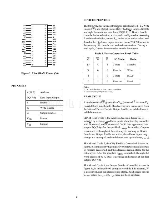
A0
A
1
A
2
A
3
A
4
A
5
A
6
A7
A
8
A9
Pre-Charge Circuit
Row Select
Memory Array
1024 Rows
512x8 Columns
I/O Circuit
Column Select
Data
Control
CLK
Gen.
A
10
A11
A
12
A
13
A
14
A
15
A
16
A
17
A
18
DQ
0
- DQ
7
E
W
G
Figure 1. UT8Q512 SRAM Block Diagram


 1
1
 2
2
 3
3
 4
4
 5
5
 6
6
 7
7
 8
8
 9
9
 10
10
 11
11
 12
12
 13
13
 14
14
 15
15
