Standard Products
UT54LVDS032LV Low Voltage Quad Receiver
Data Sheet
January 21, 2002
FEATURES
q
q
q
q
q
q
q
q
q
>400.0 Mbps (200 MHz) switching rates
+340mV differential signaling
3.3 V power supply
TTL compatible outputs
Cold spare all pins
Ultra low power CMOS technology
3.3ns maximum propagation delay
0.35ns maximum differential skew
Radiation-hardened design; total dose irradiation testing to
MIL-STD-883 Method 1019
- Total-dose: 300 krad(Si) and 1Mrad(Si)
- Latchup immune (LET > 100 MeV-cm
2
/mg)
Packaging options:
- 16-lead flatpack (dual in-line)
Standard Microcircuit Drawing 5962-98652
- QML Q and V compliant part
Compatible with IEEE 1596.3SCI LVDS
Compatible with ANSI/TIA/EIA 644-1996 LVDS
Standard
INTRODUCTION
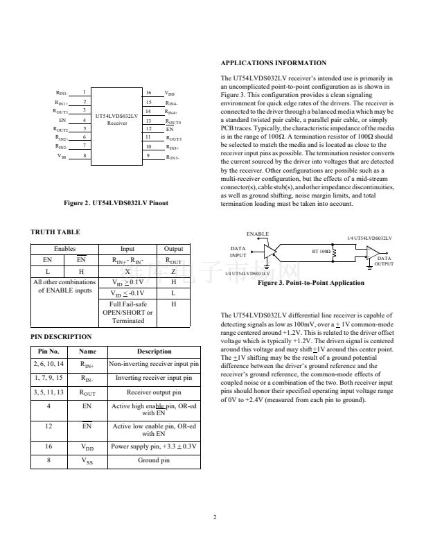
The UT54LVDS032LV Quad Receiver is a quad CMOS
differential line receiver designed for applications requiring
ultra low power dissipation and high data rates. The device is
designed to support data rates in excess of 400.0 Mbps (200
MHz) utilizing Low Voltage Differential Signaling (LVDS)
technology.
The UT54LVDS032LV accepts low voltage (340mV)
differential input signals and translates them to 5V TTL o utput
levels. The receiver supports a three-state function that may be
used to multiplex outputs. The receiver also supports OPEN,
shorted and terminated (100
鈩?
input fail-safe. Receiver output
will be HIGH for all fail-safe conditions.
The UT54LVDS032LV and companion quad line driver
UT54LVDS031LV provides new alternatives to high power
pseudo-ECL devices for high speed point-to-point interface
applications.
All pins have Cold Spare buffers. These buffers will be high
impedance when V
DD
is tied to V
SS
.
q
q
q
q
R
IN1+
R
IN1-
+
R1
-
R
OUT1
R
IN2+
R
IN2-
+
R2
-
R
OUT2
R
IN3+
R
IN3-
+
R3
-
R
OUT3
R
IN4+
R
IN4-
EN
+
R4
-
R
OUT4
EN
Figure 1. UT54LVDS032LV Quad Receiver Block Diagram
1


 1
1
 2
2
 3
3
 4
4
 5
5
 6
6
 7
7
 8
8
 9
9
 10
10
 11
11
