DATA SHEET
MOS INTEGRATED CIRCUIT
碌
PD4482162, 4482182, 4482322, 4482362
8M-BIT CMOS SYNCHRONOUS FAST SRAM
PIPELINED OPERATION
SINGLE CYCLE DESELECT
Description
The
碌
PD4482162 is a 524,288-word by 16-bit, the
碌
PD4482182 is a 524,288-word by 18-bit,
碌
PD4482322 is a 262,144-
word by 32-bit and the
碌
PD4482362 is a 262,144-word by 36-bit synchronous static RAM fabricated with advanced CMOS
technology using Full-CMOS six-transistor memory cell.
The
碌
PD4482162,
碌
PD4482182,
碌
PD4482322 and
碌
PD4482362 integrates unique synchronous peripheral circuitry, 2-
bit burst counter and output buffer as well as SRAM core. All input registers are controlled by a positive edge of the single
clock input (CLK).
The
碌
PD4482162,
碌
PD4482182,
碌
PD4482322 and
碌
PD4482362 are suitable for applications which require synchronous
operation, high speed, low voltage, high density and wide bit configuration, such as cache and buffer memory.
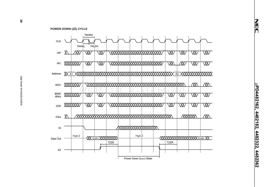
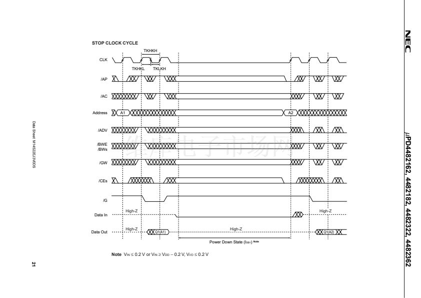
ZZ has to be set LOW at the normal operation. When ZZ is set HIGH, the SRAM enters Power Down State (鈥淪leep鈥?. In
the 鈥淪leep鈥?state, the SRAM internal state is preserved. When ZZ is set LOW again, the SRAM resumes normal operation.
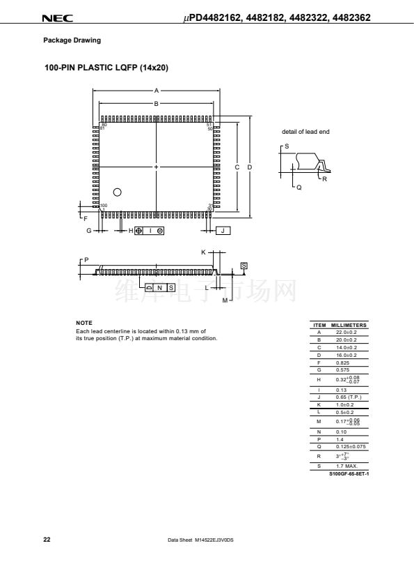
The
碌
PD4482162,
碌
PD4482182,
碌
PD4482322 and
碌
PD4482362 are packaged in 100-pin PLASTIC LQFP with a 1.4
mm package thickness for high density and low capacitive loading.
Features
鈥?/div>
3.3 V or 2.5 V core supply
鈥?/div>
Synchronous operation
鈥?/div>
Operating temperature : T
A
= 0 to 70
擄C
(-A44, -A50, -A60, -C60)
T
A
=
鈭?0
to
+85 擄C
(-A44Y, -A50Y, -A60Y, -C60Y)
鈥?/div>
Internally self-timed write control
鈥?/div>
Burst read / write : Interleaved burst and linear burst sequence
鈥?/div>
Fully registered inputs and outputs for pipelined operation
鈥?/div>
Single-Cycle deselect timing
鈥?/div>
All registers triggered off positive clock edge
鈥?/div>
3.3 V or 2.5 V LVTTL Compatible : All inputs and outputs
鈥?/div>
Fast clock access time : 2.8 ns (225 MHz), 3.1 ns (200 MHz), 3.5 ns (167 MHz)
鈥?/div>
Asynchronous output enable : /G
鈥?/div>
Burst sequence selectable : MODE
鈥?/div>
Sleep mode : ZZ (ZZ = Open or Low : Normal operation)
鈥?/div>
Separate byte write enable : /BW1 to /BW4, /BWE (
碌
PD4482322,
碌
PD4482362)
/BW1, /BW2, /BWE (
碌
PD4482162,
碌
PD4482182)
Global write enable : /GW
鈥?/div>
Three chip enables for easy depth expansion
鈥?/div>
Common I/O using three state outputs
The information in this document is subject to change without notice. Before using this document, please
confirm that this is the latest version.
Not all products and/or types are available in every country. Please check with an NEC Electronics
sales representative for availability and additional information.
Document No. M14522EJ3V0DS00 (3rd edition)
Date Published December 2002 NS CP(K)
Printed in Japan
The mark
shows major revised points.
2000
UPD4482182GF-A50Y相關(guān)型號(hào)PDF文件下載
-
型號(hào)
版本
描述
廠商
下載
-
英文版
ETC
-
英文版
ETC
-
英文版
ETC
-
英文版
ETC
-
英文版
ETC
-
英文版
2,048 x 8-BIT STATIC CMOS RAM
-
英文版
ETC
-
英文版
ETC
-
英文版
UPD4016_NEC.pdf
-
英文版
ETC
-
英文版
ETC
-
英文版
8,192 x 8-BIT NMOS XRAM
NEC [NEC]
-
英文版
ETC
-
英文版
x8 SRAM
ETC
-
英文版
x8 SRAM
ETC
-
英文版
INCREMENTAL ENCODER 8-BIT UP/DOWN COUNTER CMOS INTEGRATED CI...
-
英文版
INCREMENTAL ENCODER 8-BIT UP/DOWN COUNTER CMOS INTEGRATED CI...
NEC [NEC]
-
英文版
EXTENSION 8-BIT UP/DOWN COUNTER CMOS INTEGRATED CIRCUITS
-
英文版
EXTENSION 8-BIT UP/DOWN COUNTER CMOS INTEGRATED CIRCUITS
NEC [NEC]
-
英文版
RS-232 LINE DRIVER/RECEIVER AT 3.3 V/5 V


 1
1
 2
2
 3
3
 4
4
 5
5
 6
6
 7
7
 8
8
 9
9
 10
10
 11
11
 12
12
 13
13
 14
14
 15
15
 16
16
 17
17
 18
18
 19
19
 20
20
 21
21
 22
22
 23
23
 24
24
 25
25
 26
26
 27
27
 28
28
