PRELIMINARY DATA SHEET
碌
PA836TF
NPN SILICON EPITAXIAL TRANSISTOR (WITH 2 DIFFERENT ELEMENTS)
IN A 6-PIN THIN-TYPE SMALL MINI MOLD PACKAGE
Silicon Transistor
DESCRIPTION
The
碌
PA836TF has two different built-in transistors (Q1
and Q2) for low noise amplification in the VHF band to UHF
band.
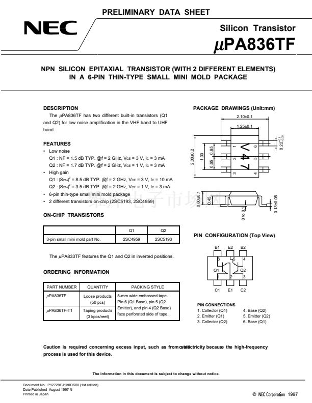
PACKAGE DRAWINGS (Unit:mm)
2.10鹵0.1
1.25鹵0.1
0.22
鈭?.05
+0.1
1
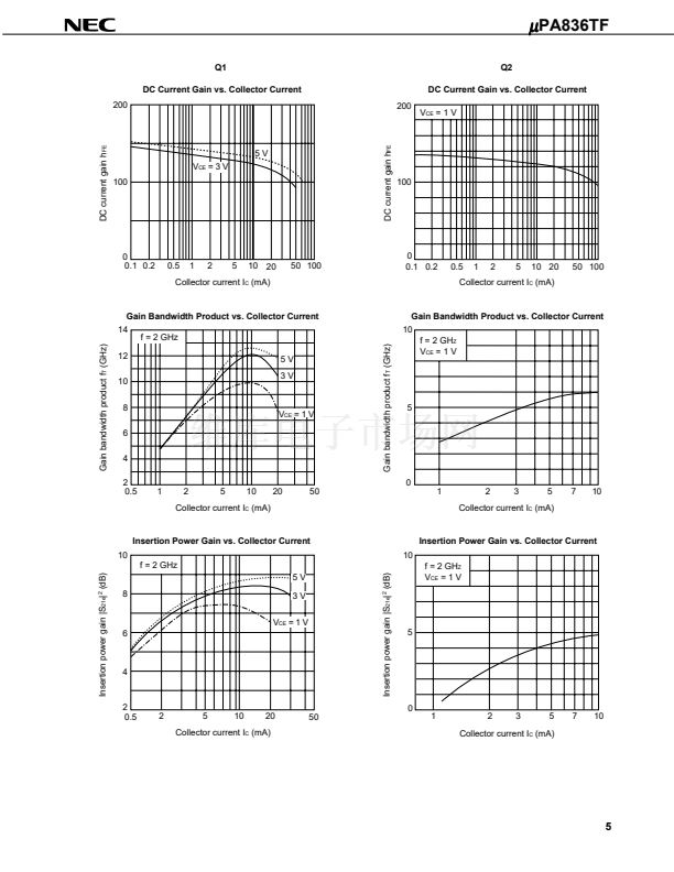
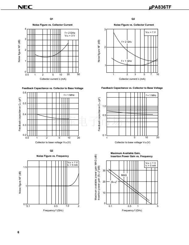
Q2 : NF = 1.7 dB TYP. @f = 2 GHz, V
CE
= 1 V, I
C
= 3 mA
鈥?High gain
Q1 :
|S
21e
|
2
= 8.5 dB TYP. @f = 2 GHz, V
CE
= 3 V, I
C
= 10 mA
Q2 :
|S
21e
|
2
= 3.5 dB TYP. @f = 2 GHz, V
CE
= 1 V, I
C
= 3 mA
鈥?2 different transistors on-chip (2SC5193, 2SC4959)
鈥?6-pin thin-type small mini mold package
0.65
Q1 : NF = 1.5 dB TYP. @f = 2 GHz, V
CE
= 3 V, I
C
= 3 mA
1.30
鈥?Low noise
2.00鹵0.2
0.65
2
3
0.60鹵0.1
4
5
6
FEATURES
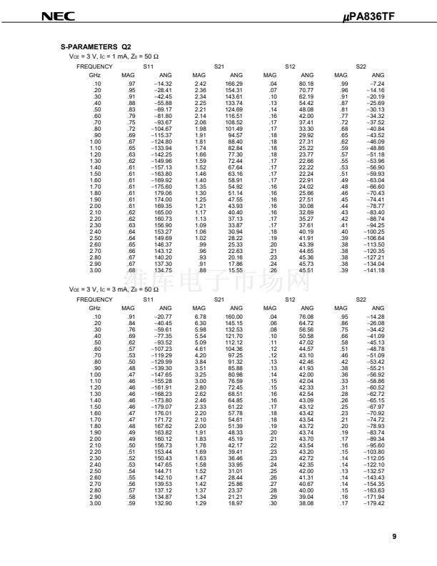
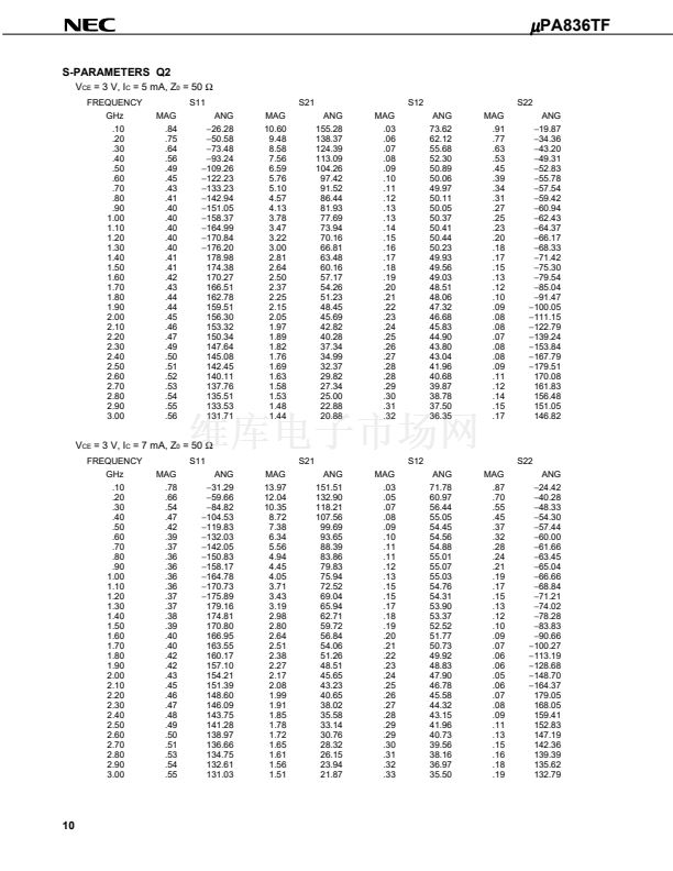
ON-CHIP TRANSISTORS
Q1
3-pin small mini mold part No.
2SC4959
Q2
2SC5193
PIN CONFIGURATION (Top View)
B1
E2
5
B2
4
Q2
2
E1
3
C2
The
碌
PA833TF features the Q1 and Q2 in inverted positions.
6
Q1
1
ORDERING INFORMATION
PART NUMBER
QUANTITY
Loose products
(50 pcs)
Taping products
(3 kpcs/reel)
PACKING STYLE
8-mm wide embossed tape.
Pin 6 (Q1 Base), pin 5 (Q2
Emitter), and pin 4 (Q2 Base)
face perforated side of tape.
C1
碌
PA836TF
碌
PA836TF-T1
PIN CONNECTIONS
1. Collector (Q1)
2. Emitter (Q1)
3. Collector (Q2)
Caution is required concerning excess input, such as from cstati
electricity becaus the high-frequency
,
e
process is used for this device.
The information in this document is subject to change without notice.
Document No. P12728EJ1V0DS00 (1st edition)
Date Published August 1997 N
Printed in Japan
0 to 0.1
4. Base (Q2)
5. Emitter (Q2)
6. Base (Q1)
漏
0.13鹵0.05
V47
0.45
1997


 1
1
 2
2
 3
3
 4
4
 5
5
 6
6
 7
7
 8
8
 9
9
 10
10
 11
11
 12
12
