鈥?/div>
6-PIN THIN-TYPE SMALL MINI MOLD PACKAGE
2 DIFFERENT BUILT-IN TRANSISTORS
(Q
1
: NE685, Q
2
: NE856)
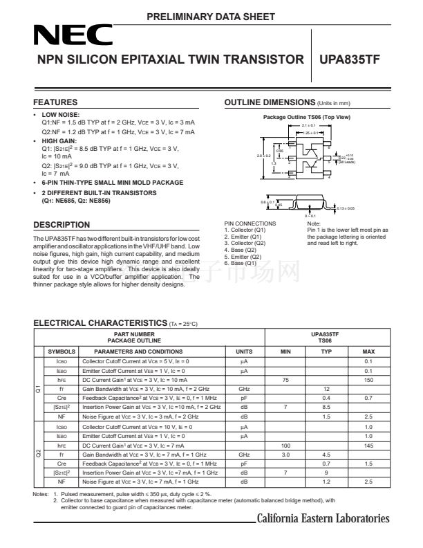
OUTLINE DIMENSIONS
(Units in mm)
Package Outline TS06 (Top View)
2.1
鹵
0.1
1.25
鹵
0.1
0.65
2.0
鹵
0.2
1.3
1
6
0.22
- 0.05
(All Leads)
+0.10
2
5
3
4
0.6
鹵
0.1
0.45
0 ~ 0.1
0.13
鹵
0.05
DESCRIPTION
The UPA835TF has two different built-in transistors for low cost
amplifier and oscillator applications in the VHF/UHF band. Low
noise figures, high gain, high current capability, and medium
output give this device high dynamic range and excellent
linearity for two-stage amplifiers. This device is also ideally
suited for use in a VCO/buffer amplifier application. The
thinner package style allows for higher density designs.
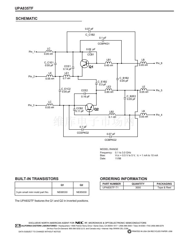
PIN CONNECTIONS
1. Collector (Q1)
2. Emitter (Q1)
3. Collector (Q2)
4. Base (Q2)
5. Emitter (Q2)
6. Base (Q1)
Note:
Pin 1 is the lower left most pin as
the package lettering is oriented
and read left to right.
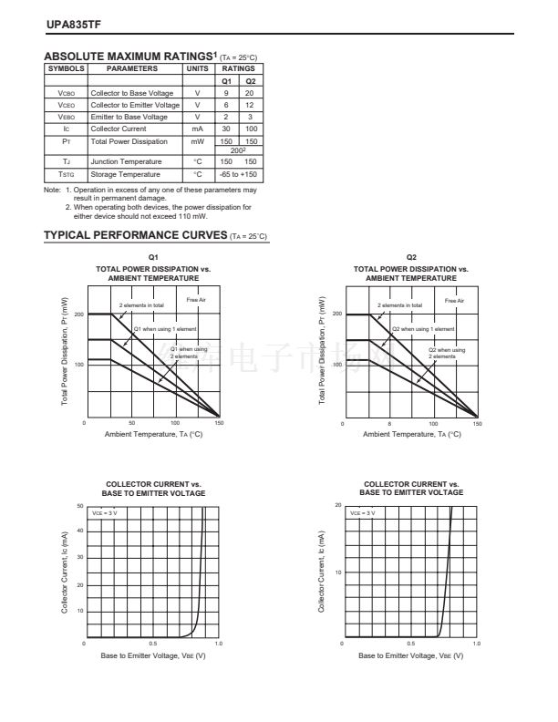
ELECTRICAL CHARACTERISTICS
(T
A
= 25擄C)
PART NUMBER
PACKAGE OUTLINE
SYMBOLS
I
CBO
I
EBO
h
FE
Q1
f
T
Cre
|S
21E
|
2
NF
I
CBO
I
EBO
h
FE
Q2
f
T
Cre
|S
21E
|
2
NF
PARAMETERS AND CONDITIONS
Collector Cutoff Current at V
CB
= 5 V, I
E
= 0
Emitter Cutoff Current at V
EB
= 1 V, I
C
= 0
DC Current
Feedback
Gain
1
at
V
CE
= 3 V, I
C
= 10 mA
GHz
pF
dB
dB
碌A(chǔ)
碌A(chǔ)
100
GHz
pF
dB
dB
7
3.0
4.5
0.7
9
1.2
2.5
1.5
7
at V
CB
= 3 V, I
E
= 0, f = 1 MHz
Gain Bandwidth at V
CE
= 3 V, I
C
= 10 mA, f = 2 GHz
Capacitance
2
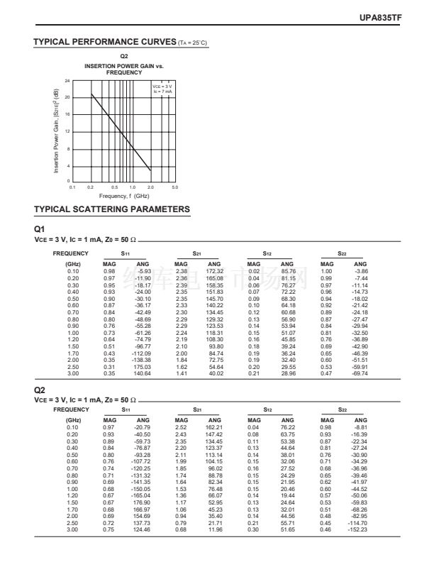
Insertion Power Gain at V
CE
= 3 V, I
C
=10 mA, f = 2 GHz
Noise Figure at V
CE
= 3 V, I
C
= 3 mA, f = 2 GHz
Collector Cutoff Current at V
CB
= 10 V, I
E
= 0
Emitter Cutoff Current at V
EB
= 1 V, I
C
= 0
DC Current Gain
1
at V
CE
= 3 V, I
C
= 7 mA
Gain Bandwidth at V
CE
= 3 V, I
C
= 7 mA, f = 1 GHz
Feedback
Capacitance
2
at V
CB
= 3 V, I
E
= 0, f = 1 MHz
Insertion Power Gain at V
CE
= 3 V, I
C
=7 mA, f = 1 GHz
Noise Figure at V
CE
= 3 V, I
C
= 7 mA, f = 1 GHz
UNITS
碌A(chǔ)
碌A(chǔ)
75
12
0.4
8.5
1.5
2.5
1.0
1.0
145
0.7
MIN
UPA835TF
TS06
TYP
MAX
0.1
0.1
150
Notes: 1. Pulsed measurement, pulse width
鈮?/div>
350
碌s,
duty cycle
鈮?/div>
2 %.
2. Collector to base capacitance when measured with capacitance meter (automatic balanced bridge method), with
emitter connected to guard pin of capacitances meter.
California Eastern Laboratories


 1
1
 2
2
 3
3
 4
4
 5
5
 6
6
 7
7
 8
8
 9
9
 10
10
