PRELIMINARY DATA SHEET
碌
PA833TF
NPN SILICON EPITAXIAL TRANSISTOR (WITH 2 DIFFERENT ELEMENTS)
IN A 6-PIN THIN-TYPE SMALL MINI MOLD PACKAGE
Silicon Transistor
DESCRIPTION
The
碌
PA833TF has two different built-in transistors (Q1
and Q2) for low noise amplification in the VHF band to UHF
band.
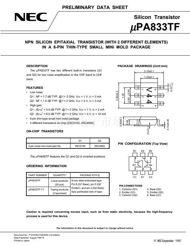
PACKAGE DRAWINGS (Unit:mm)
2.10鹵0.1
1.25鹵0.1
0.22
鈭?.05
+0.1
1
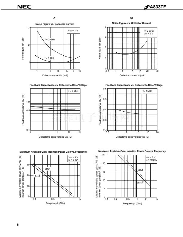
Q2 : NF = 1.5 dB TYP. @ f = 2 GHz, V
CE
= 3 V, I
C
= 3 mA
鈥?High gain
Q1 :
|S
21e
|
2
= 3.5 dB TYP. @ f = 2 GHz, V
CE
= 1 V, I
C
= 3 mA
Q2 :
|S
21e
|
2
= 8.5 dB TYP. @ f = 2 GHz, V
CE
= 3 V, I
C
= 10 mA
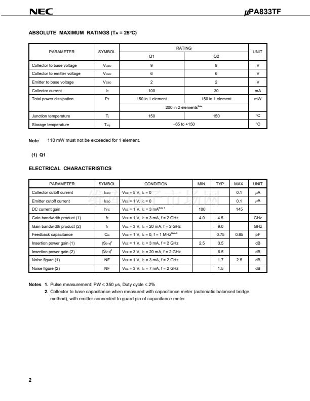
鈥?2 different transistors on-chip (2SC5193, 2SC4959)
鈥?6-pin thin-type small mini mold package
0.65
Q1 : NF = 1.7 dB TYP. @ f = 2 GHz, V
CE
= 1 V, I
C
= 3 mA
1.30
鈥?Low noise
2.00鹵0.2
0.65
2
3
0.60鹵0.1
4
5
6
FEATURES
ON-CHIP TRANSISTORS
Q1
3-pin small mini mold part No.
2SC5193
Q2
2SC4959
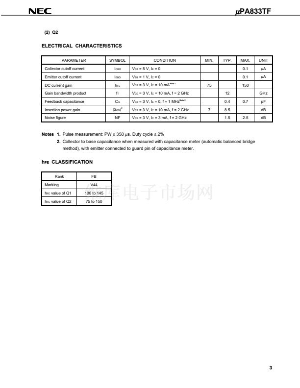
PIN CONFIGURATION (Top View)
B1
E2
5
B2
4
Q2
2
E1
3
C2
The
碌
PA836TF features the Q1 and Q2 in inverted positions.
6
Q1
1
ORDERING INFORMATION
PART NUMBER
QUANTITY
Loose products
(50 pcs)
Taping products
(3 kpcs/reel)
PACKING STYLE
8-mm wide embossed tape.
Pin 6 (Q1 Base), pin 5 (Q2
Emitter), and pin 4 (Q2 Base)
face perforated side of tape.
C1
碌
PA833TF
碌
PA833TF-T1
PIN CONNECTIONS
1. Collector (Q1)
2. Emitter (Q1)
3. Collector (Q2)
4. Base (Q2)
5. Emitter (Q2)
6. Base (Q1)
Caution is required concerning excess input, such as from static electricity, because the high-frequency
process is used for this device.
The information in this document is subject to change without notice.
Document No. P12725EJ1V0DS00 (1st edition)
Date Published August 1997 N
Printed in Japan
0 to 0.1
漏
0.13鹵0.05
V44
0.45
1997


 1
1
 2
2
 3
3
 4
4
 5
5
 6
6
 7
7
 8
8
 9
9
 10
10
 11
11
 12
12
 13
13
 14
14
 15
15
 16
16
