TSM3460
20V N-Channel MOSFET w/ESD Protected
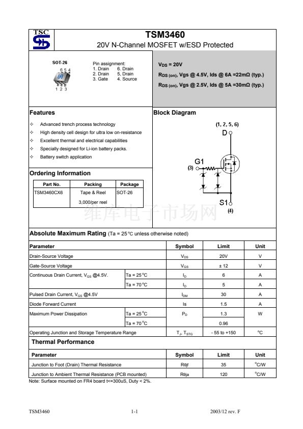
Pin assignment:
1. Drain
6. Drain
2. Drain
5, Drain
3. Gate
4. Source
V
DS
= 20V
R
DS (on)
, Vgs @ 4.5V, Ids @ 6A =22m鈩?(typ.)
R
DS (on)
, Vgs @ 2.5V, Ids @ 5A =30m鈩?(typ.)
Features
Advanced trench process technology
High density cell design for ultra low on-resistance
Excellent thermal and electrical capabilities
Specially designed for Li-ion battery packs.
Battery switch application
Block Diagram
Ordering Information
Part No.
TSM3460CX6
Packing
Tape & Reel
3,000/per reel
Package
SOT-26
Absolute Maximum Rating
(Ta = 25
o
C
unless otherwise noted)
Parameter
Drain-Source Voltage
Gate-Source Voltage
Continuous Drain Current, V
GS
@4.5V.
Ta = 25
o
C
Ta = 70
o
C
Pulsed Drain Current, V
GS
@4.5V
Diode Forward Current
Maximum Power Dissipation
Ta = 25
o
C
Ta = 70
o
C
Operating Junction and Storage Temperature Range
T
J
, T
STG
Symbol
V
DS
V
GS
I
D
I
D
I
DM
Is
P
D
Limit
20V
鹵 12
6
5
30
1.5
1.3
0.96
- 55 to +150
Unit
V
V
A
A
A
A
W
o
C
Thermal Performance
Parameter
Junction to Foot (Drain) Thermal Resistance
Junction to Ambient Thermal Resistance (PCB mounted)
Note: Surface mounted on FR4 board t<=300uS, Duty < 2%.
Symbol
R
胃jf
R
胃ja
Limit
35
120
Unit
o
o
C/W
C/W
TSM3460
1-1
2003/12 rev. F


 1
1
 2
2
 3
3
 4
4
 5
5
