, Vgs @ 5V, Ids @ 50mA = 4鈩?/div>
Features
Dual N-channel in package.
Advanced trench process technology
High density cell design for ultra low on-resistance
High input impedance
High speed switching
No minority carrier storage time
CMOS logic compatible input
No secondary breakdown
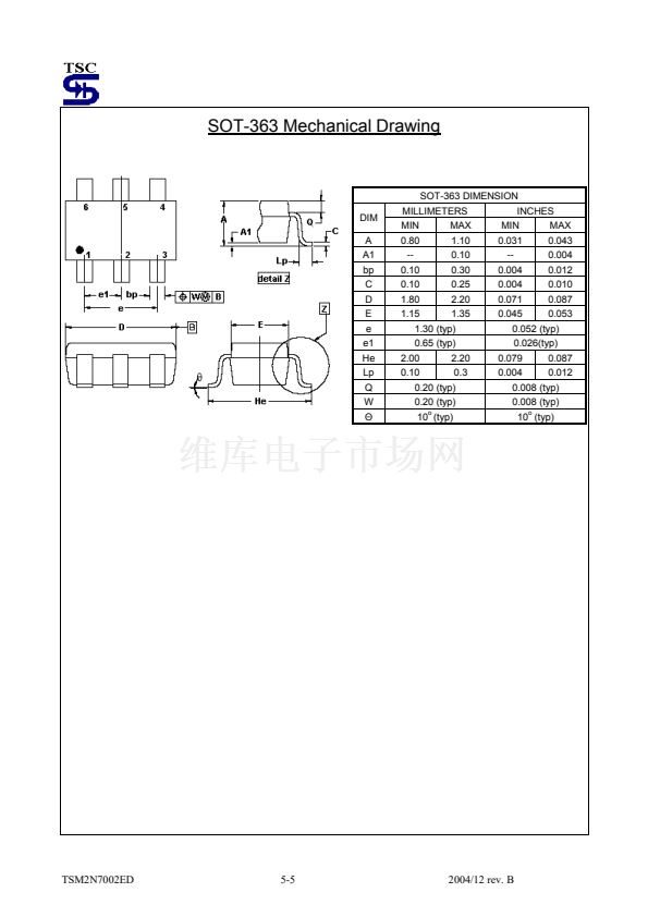
Compact and low profile SOT-363 package
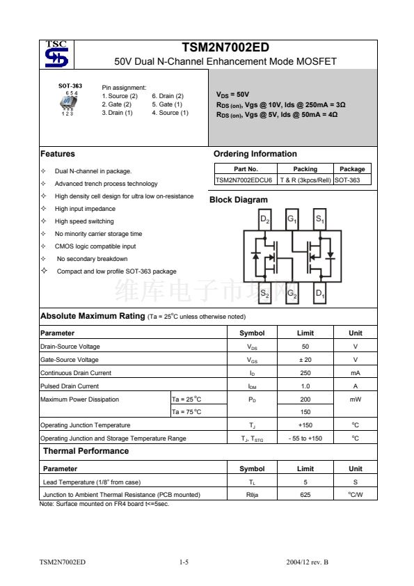
Ordering Information
Part No.
TSM2N7002EDCU6
Packing
Package
T & R (3kpcs/Rell) SOT-363
Block Diagram
Absolute Maximum Rating
(Ta = 25
o
C unless otherwise noted)
Parameter
Drain-Source Voltage
Gate-Source Voltage
Continuous Drain Current
Pulsed Drain Current
Maximum Power Dissipation
Ta = 25
o
C
Ta = 75
o
C
Operating Junction Temperature
Operating Junction and Storage Temperature Range
T
J
T
J
, T
STG
Symbol
V
DS
V
GS
I
D
I
DM
P
D
Limit
50
鹵 20
250
1.0
200
150
+150
- 55 to +150
Unit
V
V
mA
A
mW
o
o
C
C
Thermal Performance
Parameter
Lead Temperature (1/8鈥?from case)
Junction to Ambient Thermal Resistance (PCB mounted)
Note: Surface mounted on FR4 board t<=5sec.
Symbol
T
L
R
胃ja
Limit
5
625
Unit
S
o
C/W
TSM2N7002ED
1-5
2004/12 rev. B


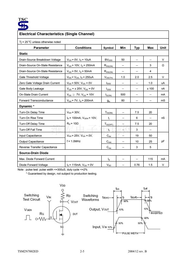
 1
1
 2
2
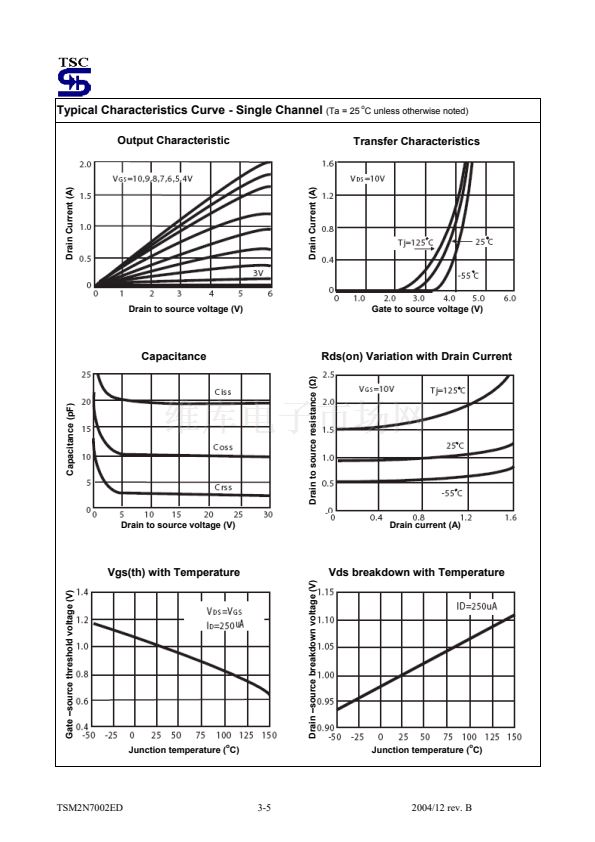 3
3
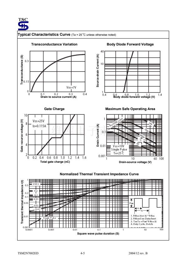 4
4
 5
5
