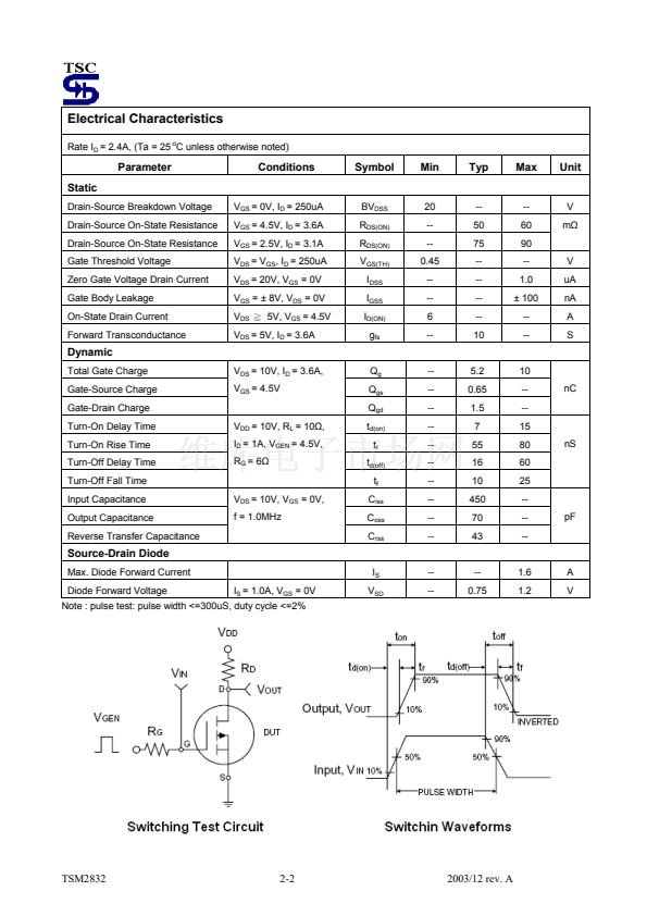
, Vgs @ 2.5V, Ids @ 3.1A = 90m鈩?/div>
Pin assignment:
1. Gate
2. Drain
3. Source
Features
Advanced trench process technology
High density cell design for ultra low on-resistance
Excellent thermal and electrical capabilities
2.5V operating voltage
Block Diagram
Ordering Information
Part No.
TSM2832CY
Packing
Tape & Reel
1kpcs per reel
Package
SOT-89
Absolute Maximum Rating
(Ta = 25鈩?/div>
Parameter
Drain-Source Voltage
Gate-Source Voltage
Continuous Drain Current
Pulsed Drain Current
Maximum Power Dissipation
unless otherwise noted)
Symbol
V
DS
V
GS
I
D
I
DM
Ta = 25
o
C
Ta = 75
o
C
P
D
Limit
20V
鹵8
3.6
10
1.5
1.0
Unit
V
V
A
A
W
Operating Junction Temperature
Operating Junction and Storage Temperature Range
T
J
T
J
, T
STG
+150
- 55 to +150
o
o
C
C
Thermal Performance
Parameter
Lead Temperature (1/8鈥?from case)
Junction to Ambient Thermal Resistance (PCB mounted)
Note: Surface mounted on FR4 board t<=5sec.
Symbol
T
L
R
胃ja
Limit
5
65
Unit
S
o
C/W
TSM2832
1-1
2003/12 rev. A


 1
1
 2
2
 3
3
 4
4
 5
5
