TSCD143K
NPN Digital Transistor
Pin assignment:
1. TR1 Gnd (Emitter)
2. TR1 Input (Base)
3. TR2 Output (Collector)
4. TR2 Gnd (Emitter)
5. TR2 Input (Base)
6. TR1 Output (Collector)
Vcc = 50V
Vin = - 5V ~ +30V
Io = 100mA(max.)
Features
Build-in bias resistor enable the configuration of an
inverter circuit without connecting external input
resistors (see equivalent circuit)
The bias resistors consist of thin-film resistors with
complete isolation to allow negative biasing of the
input. The also have the advantage of almost
completely eliminating parasitic effects.
Only the on/off conditions need to be set for operation,
making device design easy.
Two TSC143K chips in a SOT-363 package
Transistor elements are independent, eliminating
interference
Complements the TSAD143K
Equivalent Circuit
Ordering Information
Part No.
TSCD143KCU6
Packing
Tape & Reel
Package
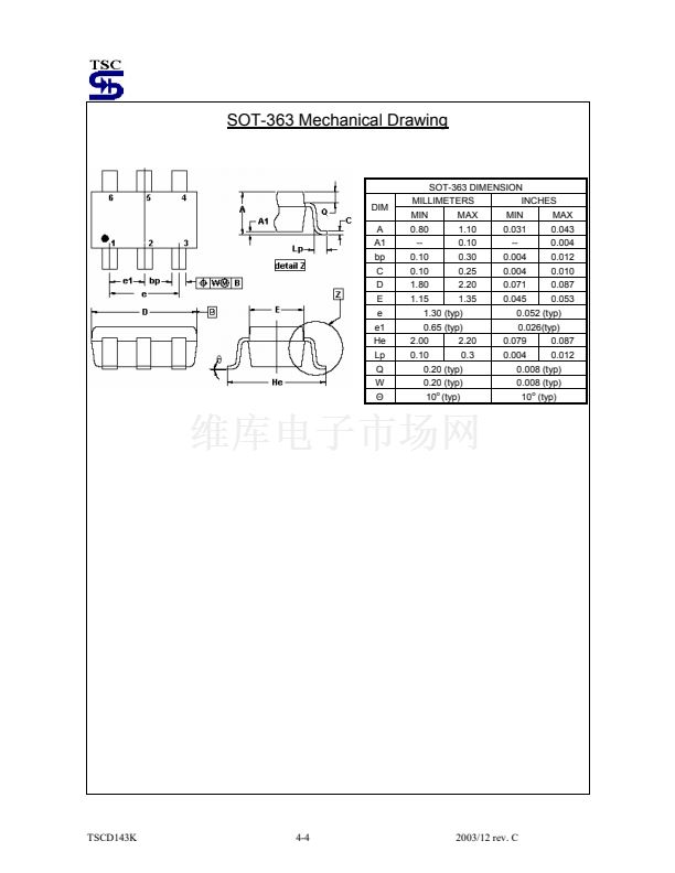
SOT-363
Note: the build-in resistor value type, option as
No.
TR 1
TR 2
Re (K鈩?
47
47
R (K鈩?
4.7
4.7
Marking
7K
Absolute Maximum Rating
(Ta = 25
o
C
unless otherwise noted)
Parameter
Supply Voltage
Input Voltage
Output Current
DC
Pulse
Power Dissipation (note)
Operating Junction Temperature
Operating Junction and Storage Temperature Range
Note: 1. Single pulse, Pw = 300uS, Duty <= 2%
2. 150mW per element must not be exceeded.
P
D
T
J
T
STG
Symbol
Vcc
Vin
Io
Limit
50
5 ~ +30
100
100
200
+150
- 55 to +150
Unit
V
V
mA
mW
o
o
C
C
TSCD143K
1-4
2003/12 rev. C


 1
1
 2
2
 3
3
 4
4
