TSC2059
General Purpose NPN Transistor
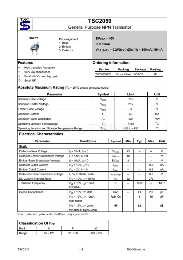
Pin assignment:
1. Base
2. Emitter
3. Collector
BV
CEO
= 40V
Ic = 50mA
V
CE (SAT)
, = 0.2V(typ.) @Ic / Ib = 500mA / 50mA
Features
High transition frequency
Very low capacitance
Small rbb鈥?Cc and high gain
Small NF.
Ordering Information
Part No.
TSC2059CX
Packing
Package
Marking
3E
3kpcs / Reel SOT-23
Absolute Maximum Rating
(Ta = 25
o
C unless otherwise noted)
Parameter
Collector-Base Voltage
Collector-Emitter Voltage
Emitter-Base Voltage
Collector Current
Collector Power Dissipation
Operating Junction Temperature
Operating Junction and Storage Temperature Range
Symbol
V
CBO
V
CEO
V
EBO
I
C
P
D
T
J
T
STG
Limit
18V
25V
3
50
225
+150
- 55 to +150
Unit
V
V
V
mA
mW
o
o
C
C
Electrical Characteristics
Parameter
Static
Collector-Base Voltage
Collector-Emitter Breakdown Voltage
Emitter-Base Breakdown Voltage
Collector Cutoff Current
Emitter Cutoff Current
Collector-Emitter Saturation Voltage
DC Current Transfer Ratio
Transition Frequency
Output Capacitance
I
C
= 10uA, I
E
= 0
I
C
= 1mA, I
B
= 0
I
E
= 10uA, I
C
= 0
V
CB
= 10V, I
E
= 0
V
EB
= 2V, I
C
= 0
I
C
/ I
B
= 20mA / 4mA
V
CE
= 10V, I
C
= 10mA
V
CE
= 10V, I
C
= 10mA,
f=200MHz
V
CB
= 10V, f=1MHz
V
CB
= 10V, I
C
= 10mA,
f=31.8MHz
V
CE
= 12V, I
C
= 2mA,
f=200MHz, Rg=50ohm
NF
--
5.5
--
dB
Cob
Rbb鈥?Cc
--
--
1.4
8
2.0
15
pF
pF
BV
CBO
BV
CEO
BV
EBO
I
CBO
I
EBO
V
CE(SAT)1
h
FE
f
T
25
18
3
--
--
--
52
--
--
--
--
--
--
--
--
1000
--
--
--
0.5
0.5
0.5
270
--
MHz
V
V
V
uA
uA
V
Conditions
Symbol
Min
Typ
Max
Unit
Note : pulse test: pulse width <=380uS, duty cycle <=2%
Classification Of h
FE
Rank
Range
K
52 - 120
P
82 - 180
Q
120 - 270
TSC2059
1-1
2004/06 rev. A


 1
1
 2
2
