TS2N2222A
General Purpose NPN Transistor
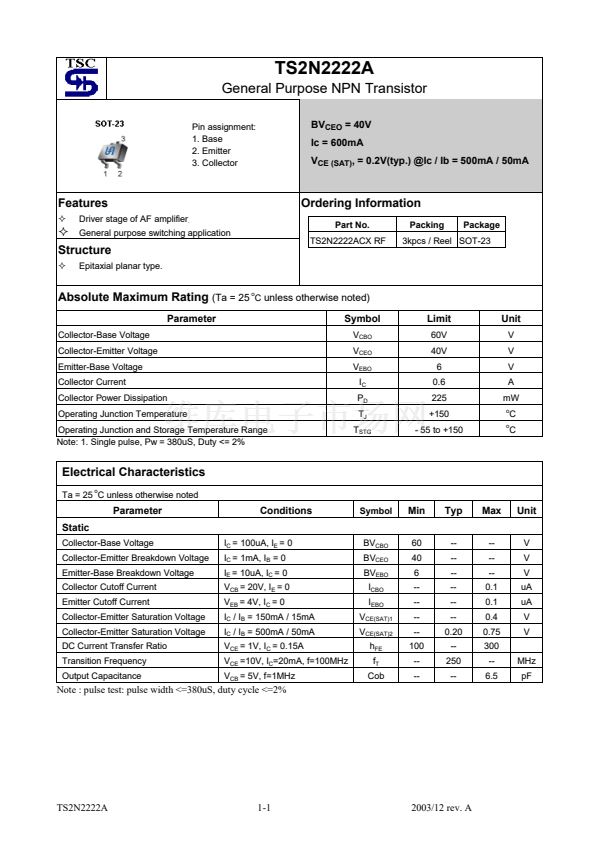
Pin assignment:
1. Base
2. Emitter
3. Collector
BV
CEO
= 40V
Ic = 600mA
V
CE (SAT)
, = 0.2V(typ.) @Ic / Ib = 500mA / 50mA
Features
Driver stage of AF amplifier
.
General purpose switching application
Ordering Information
Part No.
TS2N2222ACX RF
Packing
Package
3kpcs / Reel SOT-23
Structure
Epitaxial planar type.
Absolute Maximum Rating
(Ta = 25
o
C
unless otherwise noted)
Parameter
Collector-Base Voltage
Collector-Emitter Voltage
Emitter-Base Voltage
Collector Current
Collector Power Dissipation
Operating Junction Temperature
Operating Junction and Storage Temperature Range
Note: 1. Single pulse, Pw = 380uS, Duty <= 2%
Symbol
V
CBO
V
CEO
V
EBO
I
C
P
D
T
J
T
STG
Limit
60V
40V
6
0.6
225
+150
- 55 to +150
Unit
V
V
V
A
mW
o
o
C
C
Electrical Characteristics
Ta = 25
o
C unless otherwise noted
Parameter
Static
Collector-Base Voltage
Collector-Emitter Breakdown Voltage
Emitter-Base Breakdown Voltage
Collector Cutoff Current
Emitter Cutoff Current
Collector-Emitter Saturation Voltage
Collector-Emitter Saturation Voltage
DC Current Transfer Ratio
Transition Frequency
Output Capacitance
Conditions
I
C
= 100uA, I
E
= 0
I
C
= 1mA, I
B
= 0
I
E
= 10uA, I
C
= 0
V
CB
= 20V, I
E
= 0
V
EB
= 4V, I
C
= 0
I
C
/ I
B
= 150mA / 15mA
I
C
/ I
B
= 500mA / 50mA
V
CE
= 1V, I
C
= 0.15A
V
CE
=10V, I
C
=20mA, f=100MHz
V
CB
= 5V, f=1MHz
Symbol
Min
60
40
6
--
--
--
--
100
--
--
Typ
--
--
--
--
--
--
0.20
--
250
--
Max
--
--
--
0.1
0.1
0.4
0.75
300
--
6.5
Unit
V
V
V
uA
uA
V
V
MHz
pF
BV
CBO
BV
CEO
BV
EBO
I
CBO
I
EBO
V
CE(SAT)1
V
CE(SAT)2
h
FE
f
T
Cob
Note : pulse test: pulse width <=380uS, duty cycle <=2%
TS2N2222A
1-1
2003/12 rev. A


 1
1
 2
2
 3
3
