TRF8011
900-MHz RF TRANSMIT DRIVER
SLWS056B 鈥?FEBRUARY 1997 鈥?REVISED OCTOBER 1997
D
D
D
D
D
D
D
D
D
Operates from 4.8鈥揤 Power Supply for
900鈥揗Hz Applications
Unconditionally Stable
Wide UHF Frequency Range: 800 MHz to
1000 MHz
24.5 dBm Typical Output Power
Linear Ramp Control
Transmit Enable/Disable Control
Advanced BiCMOS Processing Technology
for Low-Power Consumption, High
Efficiency, and Highly Linear Operation
Minimum of External Components
Required for Operation
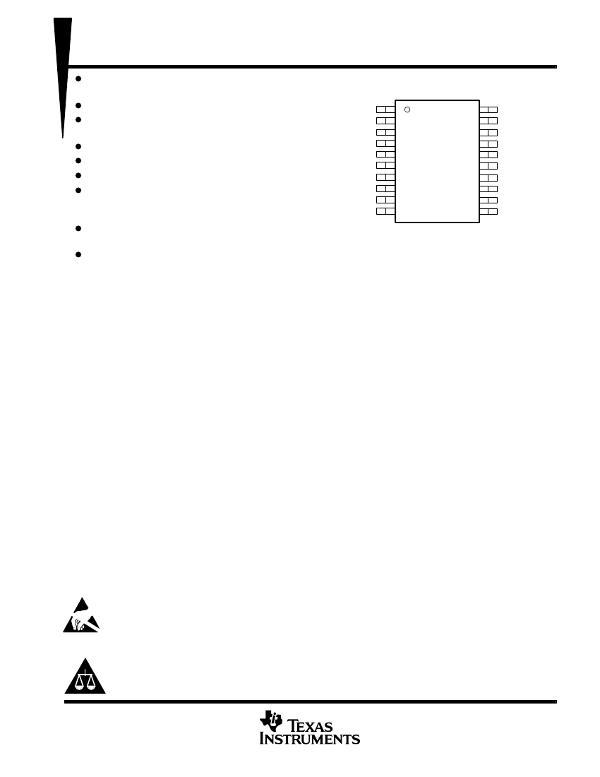
Thermally Enhanced Surface-Mount
Package for Extremely Small Circuit
Footprint
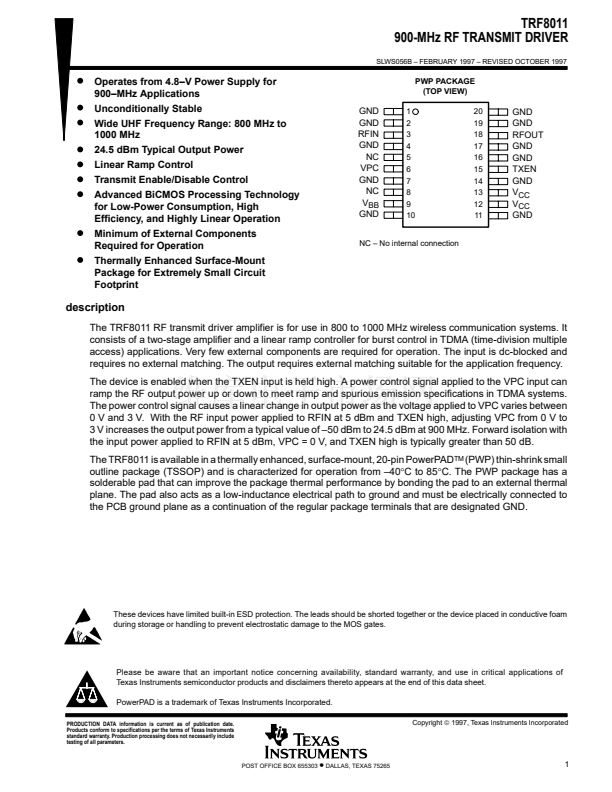
PWP PACKAGE
(TOP VIEW)
GND
GND
RFIN
GND
NC
VPC
GND
NC
V
BB
GND
1
2
3
4
5
6
7
8
9
10
20
19
18
17
16
15
14
13
12
11
GND
GND
RFOUT
GND
GND
TXEN
GND
V
CC
V
CC
GND
NC 鈥?No internal connection
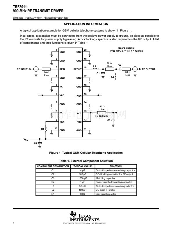
description
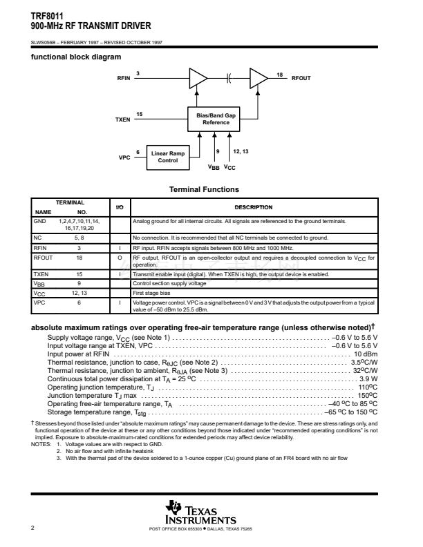
The TRF8011 RF transmit driver amplifier is for use in 800 to 1000 MHz wireless communication systems. It
consists of a two-stage amplifier and a linear ramp controller for burst control in TDMA (time-division multiple
access) applications. Very few external components are required for operation. The input is dc-blocked and
requires no external matching. The output requires external matching suitable for the application frequency.
The device is enabled when the TXEN input is held high. A power control signal applied to the VPC input can
ramp the RF output power up or down to meet ramp and spurious emission specifications in TDMA systems.
The power control signal causes a linear change in output power as the voltage applied to VPC varies between
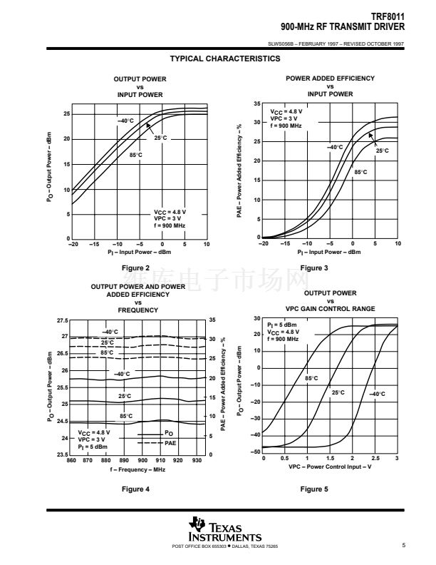
0 V and 3 V. With the RF input power applied to RFIN at 5 dBm and TXEN high, adjusting VPC from 0 V to
3 V increases the output power from a typical value of 鈥?0 dBm to 24.5 dBm at 900 MHz. Forward isolation with
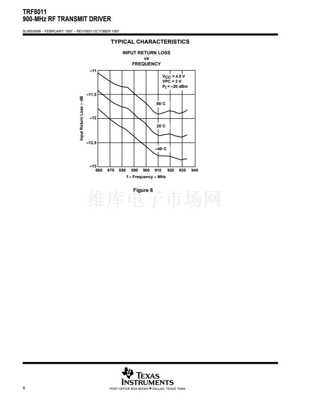
the input power applied to RFIN at 5 dBm, VPC = 0 V, and TXEN high is typically greater than 50 dB.
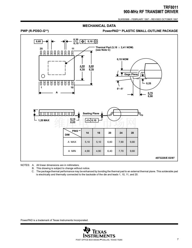
The TRF8011 is available in a thermally enhanced, surface-mount, 20-pin PowerPAD
TM
(PWP) thin-shrink small
outline package (TSSOP) and is characterized for operation from 鈥?0擄C to 85擄C. The PWP package has a
solderable pad that can improve the package thermal performance by bonding the pad to an external thermal
plane. The pad also acts as a low-inductance electrical path to ground and must be electrically connected to
the PCB ground plane as a continuation of the regular package terminals that are designated GND.
These devices have limited built-in ESD protection. The leads should be shorted together or the device placed in conductive foam
during storage or handling to prevent electrostatic damage to the MOS gates.
Please be aware that an important notice concerning availability, standard warranty, and use in critical applications of
Texas Instruments semiconductor products and disclaimers thereto appears at the end of this data sheet.
PowerPAD is a trademark of Texas Instruments Incorporated.
PRODUCTION DATA information is current as of publication date.
Products conform to specifications per the terms of Texas Instruments
standard warranty. Production processing does not necessarily include
testing of all parameters.
Copyright
漏
1997, Texas Instruments Incorporated
POST OFFICE BOX 655303
鈥?/div>
DALLAS, TEXAS 75265
1


 1
1
 2
2
 3
3
 4
4
 5
5
 6
6
 7
7
 8
8
