TPS5511
3-CHANNEL POWER SUPPLY SUPERVISOR
SLVS170 鈥?AUGUST 1998
D
D
D
D
D
D
D
D
Over Voltage Protection and Lock Out for
5 V, 3.3 V, and 12 V
Fault Protection Output with Open Drain
Output Stage
Open Drain Power Good Output Signal for
Power Good Input, 5 V and 3.3 V
300 ms Power Good Delay
2.3 ms PSON Control to FPO Turn-Off Delay
38 ms PSON Control Debounce
73
碌s
Width Noise Deglitches
Wide Power Supply Voltage Range
from 4 V to 15 V
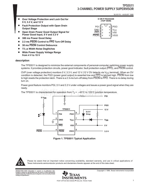
D OR P PACKAGE
(TOP VIEW)
PGI
GND
FPO
PSON
1
2
3
4
8
7
6
5
PGO
V
CC
VS5
VS33
description
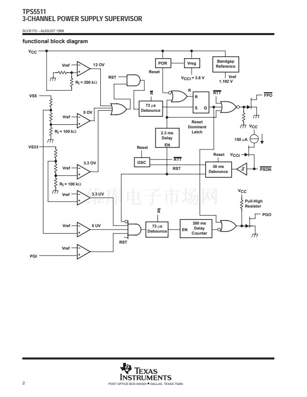
The TPS5511 is designed to minimize the external components of personal-computer switching power supply
systems. It provides protection circuits, power good indicator, fault protection output (FPO), and PSON control.
OVP (over voltage protection) monitors 5 V, 3.3 V, and 12 V (12 V OV detects via V
CC
terminal). When an OV
condition is detected, the PGO (power good output) is asserted low and FPO is latched high. PSON from low
to high resets the protection latch. There is a 2.3-ms turn-off delay from PSON to FPO. There is no delay during
turn on.
Power good feature monitors PGI, 5 V and 3.3 V under voltages and issues a power good signal when they are
ready.
The TPS5511 is characterized for operation from T
J
= 鈥?0擄C to 125擄C junction temperature.
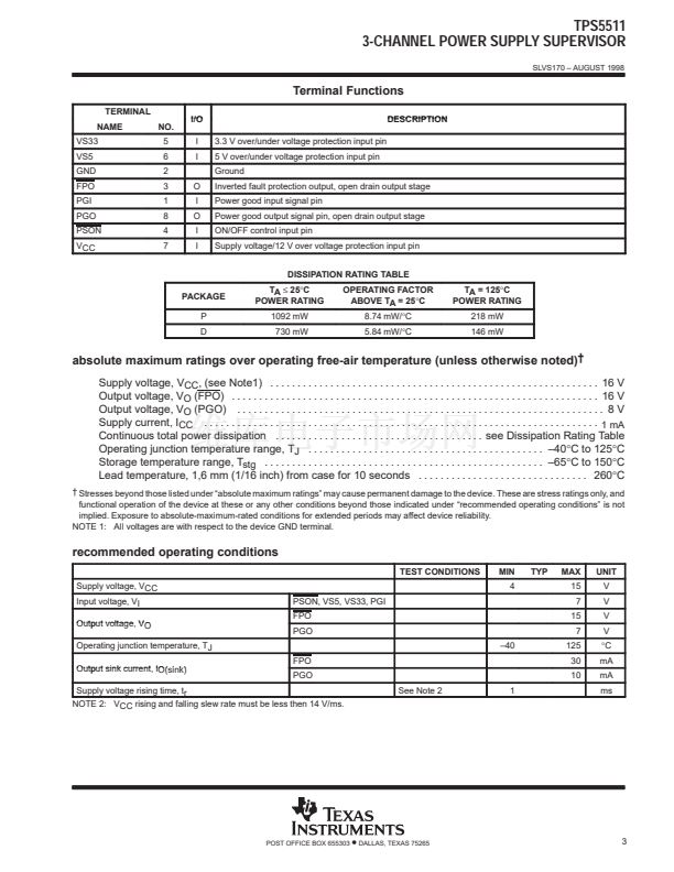
5 VSB
PGI
PGO
TPS5511
1
2
3
4
PGI
GND
FPO
PSON
PGO
VCC
VS5
VS33
8
7
6
5
0.5 V
Drop
VSB
5V
3.3 V
12 V
PSON
Figure 1. TPS5511 Typical Application
Please be aware that an important notice concerning availability, standard warranty, and use in critical applications of
Texas Instruments semiconductor products and disclaimers thereto appears at the end of this data sheet.
PRODUCTION DATA information is current as of publication date.
Products conform to specifications per the terms of Texas Instruments
standard warranty. Production processing does not necessarily include
testing of all parameters.
Copyright
漏
1998, Texas Instruments Incorporated
POST OFFICE BOX 655303
鈥?/div>
DALLAS, TEXAS 75265
1


 1
1
 2
2
 3
3
 4
4
 5
5
 6
6
 7
7
 8
8
