Avalanche Energy . . . 30 mJ
ESD Protection . . . 2500 V
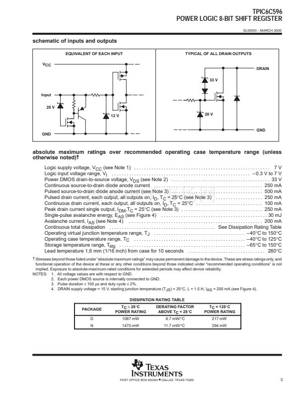
Output Clamp Voltage . . . 33 V
load power such as LEDs. The device contains a
transient protection. Power driver applications
medium-voltage loads.
鈥?/div>
G
RCK
CLR
SRCK
SER IN
8
10
7
15
2
R
EN3
C2
SRG8
C1
1D
2
3
4
5
DRAIN0
DRAIN1
DRAIN2
This device contains an 8-bit serial-in, parallel-out
6
DRAIN3
shift register that feeds an 8-bit D-type storage
11
DRAIN4
register. Data transfers through both the shift and
12
DRAIN5
storage registers on the rising edge of the shift
13
register clock (SRCK) and the register clock
DRAIN6
14
(RCK), respectively. The storage register trans-
DRAIN7
2
fers data to the output buffer when shift register
9
SER OUT
clear (CLR) is high. When CLR is low, all registers
in the device are cleared. When output enable (G)
鈥?This symbol is in accordance with ANSI/IEEE Std 91-1984
is held high, all data in the output buffers is held
and IEC Publication 617-12.
low and all drain outputs are off. When G is held
low, data from the storage register is transparent to the output buffers. When data in the output buffers is low,
the DMOS transistor outputs are off. When data is high, the DMOS transistor outputs have sink-current
capability. The serial output (SER OUT) is clocked out of the device on the falling edge of SRCK to provide
additional hold time for cascaded applications. This will provide improved performance for applications where
clock signals may be skewed, devices are not located near one another, or the system must tolerate
electromagnetic interference.
This device contains circuits to protect its inputs and outputs against damage due to high static voltages or electrostatic fields. These
circuits have been qualified to protect this device against electrostatic discharges (ESD) of up to 2 kV according to MIL-STD-883C,
Method 3015; however, it is advised that precautions be taken to avoid application of any voltage higher than maximum-rated
voltages to these high-impedance circuits. During storage or handling, the device leads should be shorted together or the device
should be placed in conductive foam. In a circuit, unused inputs should always be connected to an appropriated logic voltage level,
preferably either VCC or ground. Specific guidelines for handling devices of this type are contained in the publication
Guidelines for
Handling Electrostatic-Discharge-Sensitive (ESDS) Devices and Assemblies
available from Texas Instruments.
Please be aware that an important notice concerning availability, standard warranty, and use in critical applications of
Texas Instruments semiconductor products and disclaimers thereto appears at the end of this data sheet.
Copyright
漏
2000, Texas Instruments Incorporated
PRODUCTION DATA information is current as of publication date.
Products conform to specifications per the terms of Texas Instruments
standard warranty. Production processing does not necessarily include
testing of all parameters.
POST OFFICE BOX 655303
鈥?/div>
DALLAS, TEXAS 75265
1


 1
1
 2
2
 3
3
 4
4
 5
5
 6
6
 7
7
 8
8
 9
9
 10
10
 11
11
 12
12
