鈥?/div>
TTL-Compatible Inputs
CCD-Compatible Outputs
Variable-Output Slew Rates With External
Resistor Control
Frame-Transfer Operation
Solid-State Reliability
Adjustable Clock Levels
DW PACKAGE
(TOP VIEW)
description
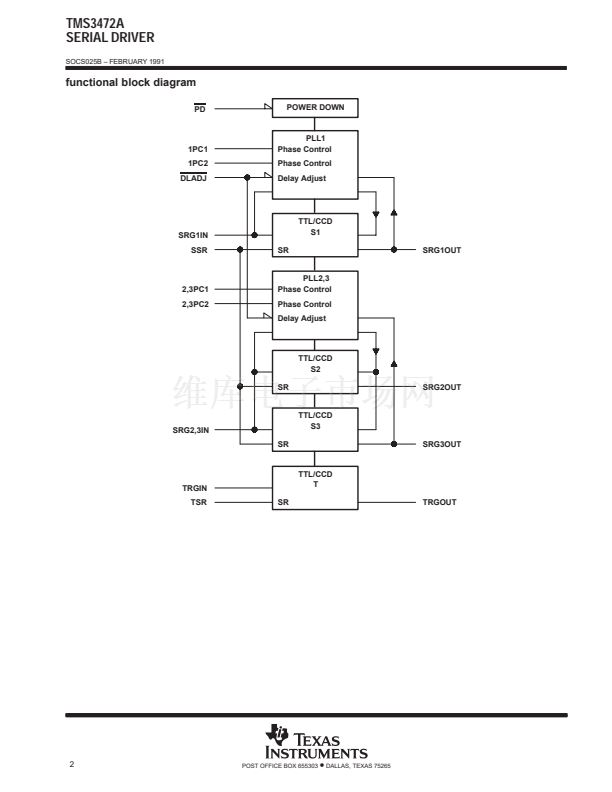
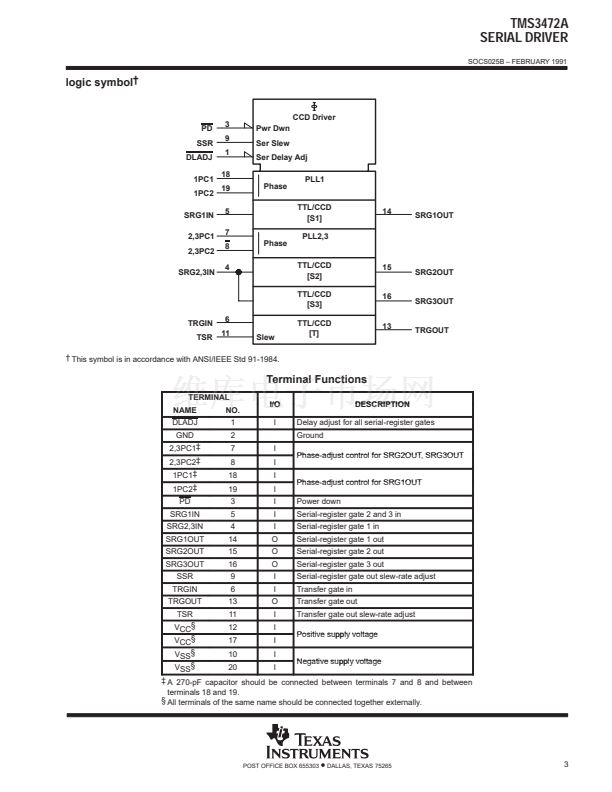
The TMS3472A serial driver is a monolithic
9
12
CMOS integrated circuit designed to drive the
10
11
serial-register gate (SRGn) and transfer-gate
(TRG) inputs of the Texas Instruments (TI鈩?
TC241 (monochrome) CCD image sensor. The TMS3472A interfaces the TI TMS3471C or a user-defined
timing generator to the TC241; it receives TTL signals from the timing generator and outputs level-shifted and
slew-rate-adjusted signals to the image sensor. The TMS3472A contains three noninverting serial drivers and
one noninverting transfer driver as well as circuitry for slew-rate adjustment.
The voltage levels on SRG1OUT, SRG2OUT, SRG3OUT, and TRGOUT are controlled by the levels on V
SS
and
V
CC
. DLADJ, PD, SRG1IN, SRG2,3IN, and TRGIN are TTL compatible. A high level on PD allows the TMS3472
to operate normally with the level-shifted and slew-rate-adjusted outputs following the inputs. When PD is low,
the device is in a low power-consumption mode and all outputs are at V
CC
.
The slew rate of SRG1OUT, SRG2OUT, and SRG3OUT is controlled by connecting a resistor between V
CC
and
SSR. The TRGOUT slew rate is controlled by connecting a resistor between V
CC
and TSR. The larger the
resistor values, the longer the rise and fall times are.
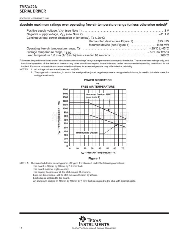
The TMS3472A is available in a 20-pin surface-mount package (DW) and is characterized for operation from
鈥?20擄C to 45擄C.
DLADJ
GND
PD
SRG2,3IN
SRG1IN
TRGIN
2,3PC1
2,3PC2
SSR
V
SS
1
2
3
4
5
6
7
8
20
19
18
17
16
15
14
13
V
SS
1PC2
1PC1
V
CC
SRG3OUT
SRG2OUT
SRG1OUT
TRGOUT
V
CC
TSR
This device contains circuits to protect its inputs and outputs against damage due to high static voltages or electrostatic fields. These
circuits have been qualified to protect this device against electrostatic discharges (ESD) of up to 2 kV according to MIL-STD-883C,
Method 3015; however, precautions should be taken to avoid application of any voltage higher than maximum-rated voltages to these
high-impedance circuits. During storage or handling, the device leads should be shorted together or the device should be placed in
conductive foam. In a circuit, unused inputs should always be connected to an appropriated logic voltage level, preferably either VCC or ground.
Specific guidelines for handling devices of this type are contained in the publication
Guidelines for Handling Electrostatic-Discharge-Sensitive
(ESDS) Devices and Assemblies
available from Texas Instruments.
TI is a trademark of Texas Instruments Incorporated.
PRODUCTION DATA information is current as of publication date.
Products conform to specifications per the terms of Texas Instruments
standard warranty. Production processing does not necessarily include
testing of all parameters.
Copyright
漏
1991, Texas Instruments Incorporated
POST OFFICE BOX 655303
鈥?/div>
DALLAS, TEXAS 75265
1


 1
1
 2
2
 3
3
 4
4
 5
5
 6
6
 7
7
 8
8
 9
9
