鈥?/div>
NTSC-Timing Operation
Solid-State Reliability
Monochrome Operation
Eight Selectable-Antiblooming Modes
Surface-Mount Package
Clamp-Pulse Select Option
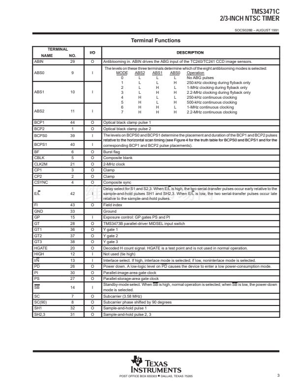
BCP2
CP2
CP1
CSYNC
CBLK
BF
SC
SC(90)
ABS0
ABS1
ABS2
1
2
3
4
5
6
7
8
9
10
11
FS PACKAGE
(TOP VIEW)
44 43 42 41 40 39 38 37 36 35 34
33
32
31
30
29
28
27
26
25
24
23
12 13 14 15 16 17 18 19 20 21 22
BCP1
FI
E/L
VDS
BCPS1
BCPS0
GT3
GT2
GT1
X2
X1
description
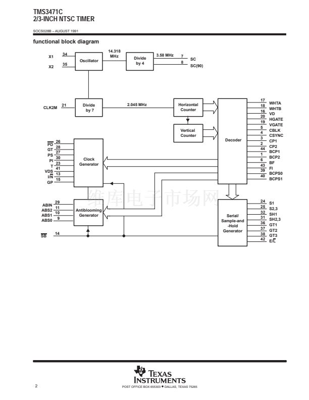
The TMS3471C is a monolithic integrated circuit
designed to supply timing signals for the Texas
Instruments (TI鈩? 11-mm diagonal TC241 mono-
chrome CCD image sensor. The TMS3471C
supplies both CCD drive signals and NTSC
television synchronization signals at standard
video rates. It requires a single 5-V supply voltage
and a 14.318-MHz crystal-oscillator input. The
TMS3471C provides several options, including
multiple antiblooming modes, clamp-pulse selec-
tion, and delayed horizontal transfer.
GND
SH1
SH2,3
PI
ABIN
GT
PS
PD
S2,3
S1
T
The TMS3471C is used in conjunction with
level-shifting devices such as the TI TMS3473B
parallel driver and the TI TMS3472A serial driver.
It also supplies sample-and-hold signals for the TI TL1593 three-channel sample-and-hold and multiplex signals
for the TI TL1051 video preprocessor. The TMS3471C NTSC synchronization-signal outputs include composite
sync, composite blank, clamp, subcarrier, subcarrier delayed by 90 degrees, and burst flag.
The TMS3471C is supplied in a 44-pin plastic flat package and is characterized for operation from 鈥?20擄C
to 45擄C.
This device contains circuits to protect its inputs and outputs against damage due to high static voltages or electrostatic fields. These
circuits have been qualified to protect this device against electrostatic discharges (ESD) of up to 2 kV according to MIL-STD-883C,
Method 3015; however, precautions should be taken to avoid application of any voltage higher than maximum-rated voltages to these
high-impedance circuits. During storage or handling, the device leads should be shorted together or the device should be placed in
conductive foam. In a circuit, unused inputs should always be connected to an appropriate logic voltage level, preferably either VCC or ground.
Specific guidelines for handling devices of this type are contained in the publication
Guidelines for Handling Electrostatic-Discharge-Sensitive
(ESDS) Devices and Assemblies
available from Texas Instruments.
TI is a trademark of Texas Instruments Incorporated.
PRODUCTION DATA information is current as of publication date.
Products conform to specifications per the terms of Texas Instruments
standard warranty. Production processing does not necessarily include
testing of all parameters.
POST OFFICE BOX 655303
鈥?/div>
DALLAS, TEXAS 75265
HIGH
I/N
SB
GP
VD
WHTA
WHTB
VGATE
HGATE
CLK2M
V CC
Copyright
漏
1991, Texas Instruments Incorporated
1


 1
1
 2
2
 3
3
 4
4
 5
5
 6
6
 7
7
 8
8
 9
9
 10
10
 11
11
 12
12
 13
13
 14
14
 15
15
 16
16
 17
17
 18
18
 19
19
