TK65015
FEATURES
s
0.9 V Operation
s
Very Low Quiescent Current
s
Internal Bandgap Reference
s
High Efficiency
s
Low Output Ripple
s
Microprocessor Reset Output
s
Laser-Trimmed Output Voltage
s
Undervoltage Lockout
s
Regulation by Pulse Burst Modulation (PBM)
STEP-UP VOLTAGE CONVERTER
WITH VOLTAGE MONITOR
APPLICATIONS
s
Battery Powered Systems
s
Cellular Telephones
s
Pagers
s
Personal Communications Equipment
s
Portable Instrumentation
s
Portable Consumer Equipment
s
Radio Control Systems
DESCRIPTION
The TK65015 Low Power Step-Up DC-DC converter is
designed for portable battery powered systems, capable of
operating from a single battery cell down to 0.9 V.
The output voltage is laser-trimmed to 3.0 V. An internal
detector monitors the output voltage and provides an
active-low microprocessor reset signal whenever the out-
put voltage falls below an internally preset limit. An internal
undervoltage lockout circuit is utilized to prevent the induc-
tor switch from remaining in the "ON" mode when the
battery voltage is too low to permit normal operation.
Special care has been taken to achieve high reliability
through the use of Oxide, Nitride passivation and an
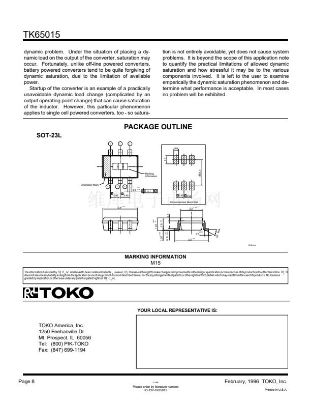
additional polyimide coating. The TK65015 is available in a
very small plastic surface mount package. (SOT-23L)
Pulse burst modulation (PBM) is used to regulate the
voltage at the V
OUT
pin at the IC. PBM is the process in
which an oscillator signal is gated or not gated to the switch
drive each period. The decision is made just before the start
of each cycle and is based on comparing the output voltage
to an internally-generated bandgap reference. The deci-
sion is latched, so the duty ratio is not modulated within a
cycle. The average duty ratio is effectively modulated by
the "bursting" and skipping of pulses which can be seen at
the IND pin of the IC.
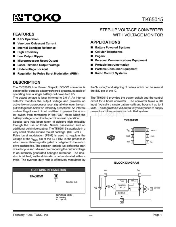
The TK65015 provides the power switch and the control
circuit for a boost converter. The converter takes a DC
input (typically a single battery cell) and boosts it up to 3
volts. This regulated 3 volt output is typically used to supply
power to a microprocessor-controlled system.
TK65015M
2
VIN
M15
1
6
5
4
RESET
GND
VO
GND 2
IND
3
BLOCK DIAGRAM
ORDERING INFORMATION
TK65015M
Tape/Reel Code
IND
3
VO
4
V
REF
VIN
CONTROL
CIRCUIT
RC OSC.
UVLO
1
6
RESET
TAPE/REEL CODE
BX : Bulk/Bag
TL : Tape Left
2,5
GND
February, 1996 TOKO, Inc.
2-2-96
Page 1


 1
1
 2
2
 3
3
 4
4
 5
5
 6
6
 7
7
 8
8
