TC1225
TC1226
TC1227
Inverting Dual (鈥揤
IN
, 鈥?V
IN
) Charge Pump Voltage Converters
FEATURES
s
s
s
s
s
s
Small 8-Pin MSOP Package
Operates from 1.8V to 5.5V
Up to 5mA Output Current at 鈥揤
IN
Pin
Up to 1mA Output Current at 鈥?V
IN
Pin
鈥揤
IN
and 鈥?V
IN
Outputs Available
Low Supply Current
.......................................... 120
碌
A (MAX) for TC1225
.......................................... 360
碌
A (MAX) for TC1226
.......................................... 1.5mA (MAX) for TC1227
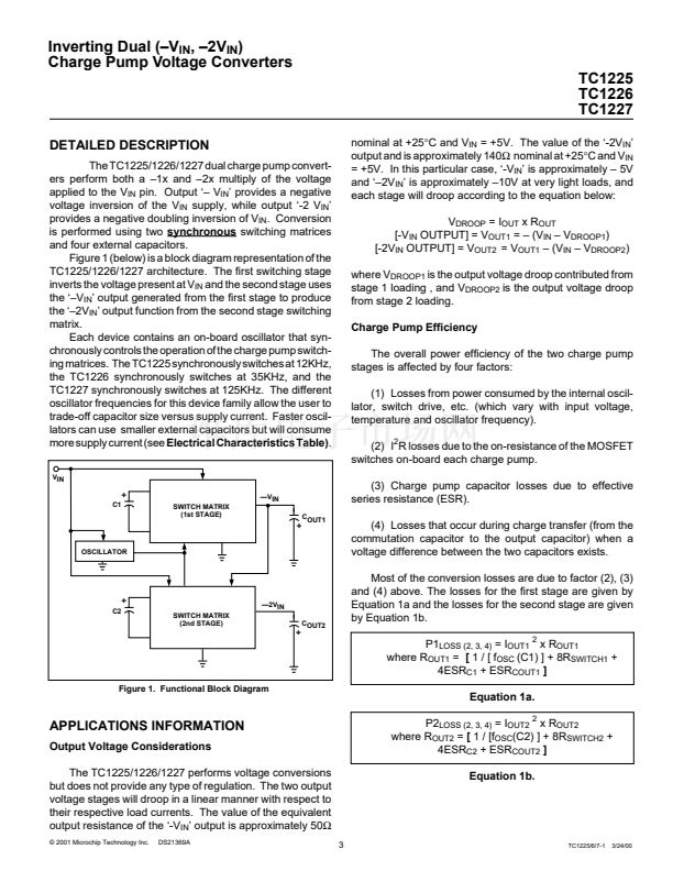
GENERAL DESCRIPTION
The TC1225/1226/1227 are CMOS dual inverting charge
pump voltage converters in 8-Pin MSOP packages. An on-
board oscillator provides the clock, and only four external
capacitors are required for full circuit implementation. Switch-
ing frequencies are 12kHz for the TC1225, 35kHz for the
TC1226, and 125kHz for the TC1227.
These devices provide both a negative voltage inversion
(available at the 鈥揤
IN
output) and a negative doubling
voltage inversion (available at the 鈥? V
IN
output), with a low
output impedance capable of providing output currents up to
5mA for the 鈥揤
IN
output and 1mA for the 鈥?V
IN
output. The
input voltage can range from +1.8V to +5.5V.
TYPICAL APPLICATIONS
s
s
s
s
s
LCD Panel Bias
Cellular Phones PA Bias
Pagers
PDAs, Portable Data loggers
Battery Powered Devices
ORDERING INFORMATION
Part No.
TC1225EUA
TC1226EUA
TC1227EUA
Package Osc Freq (kHz) Temp Range
8-Pin MSOP
8-Pin MSOP
8-Pin MSOP
12
35
125
鈥?0擄C to +85擄C
鈥?0擄C to +85擄C
鈥?0擄C to +85擄C
TYPICAL OPERATING CIRCUIT
C1+
C1鈥?/div>
C2+
+
C1
V
IN
鈥揤
IN
INPUT
OUTPUT 1
PIN CONFIGURATION
8-Pin MSOP
C1鈥?/div>
C2+
C2鈥?/div>
1
2
3
4
TC1225
TC1226
TC1227
8 鈥揤
IN
7
C1+
+
C2
TC1225
TC1226
C2鈥?TC1227
GND
鈥?C
OUT1
+
6 V
IN
5
GND
鈥? V
IN
鈥?C
OUT2
+
OUTPUT 2
鈥?V
IN
Notes:
1) C1 and C
OUT1
must have a voltage rating greater
than or equal to V
IN
2) C2 and C
OUT2
must have a voltage rating greater
than or equal to 2V
IN
漏 2001 Microchip Technology Inc.
DS21369A
TC1225/6/7-1
3/24/00


 1
1
 2
2
 3
3
 4
4
 5
5
 6
6
 7
7
 8
8
 9
9
 10
10
