鈥?/div>
RECALL
to SRAM Initiated by Software or
Power Restore
鈥?10mA Typical I
CC
at 200ns Cycle Time
鈥?Unlimited READ, WRITE and
RECALL
Cycles
鈥?1,000,000
STORE
Cycles to EEPROM
鈥?100-Year Data Retention over Full Industrial
Temperature Range
鈥?Commercial and Industrial Temperatures
鈥?24-Pin 600 PDIP Package
DESCRIPTION
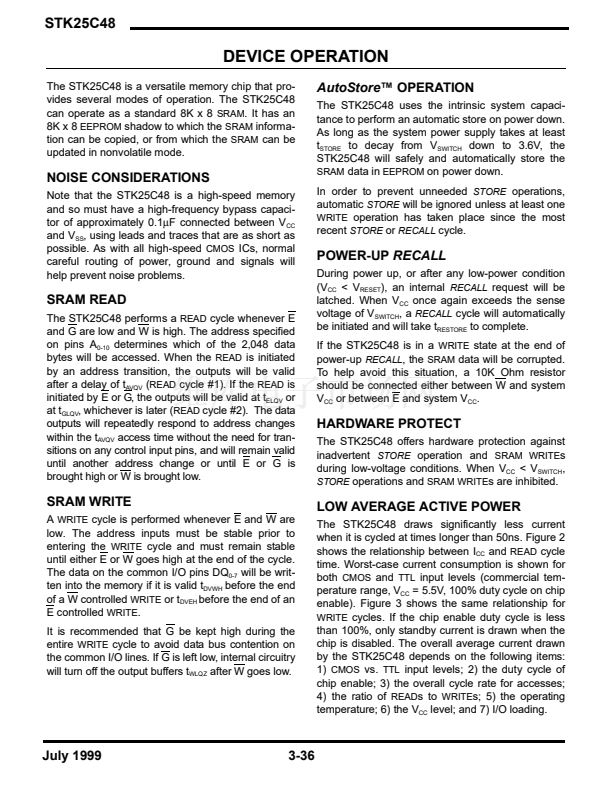
The STK25C48 is a fast
SRAM
with a nonvolatile
EEPROM
element incorporated in each static memory
cell. The
SRAM
can be read and written an unlimited
number of times, while independent nonvolatile data
resides in the
EEPROM.
Data transfers from the
SRAM
to
the
EEPROM
(the
STORE
operation) can take place auto-
matically on power down using charge stored in system
capacitance. Transfers from the
EEPROM
to the
SRAM
(the
RECALL
operation) take place automatically on res-
toration of power. The nvSRAM can be used in place of
existing 2K x 8
SRAMs
and also matches the pinout of
2K x 8 battery-backed
SRAMs, EPROMs
and
EEPROMs,
allowing direct substitution while enhancing performance.
There is no limit on the number of read or write cycles that
can be executed, and no support circuitry is required for
microprocessor interfacing.
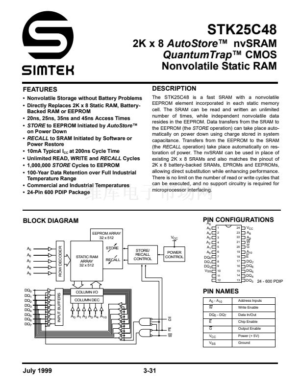
BLOCK DIAGRAM
EEPROM ARRAY
32 x 512
ROW DECODER
V
CC
STORE/
RECALL
CONTROL
PIN CONFIGURATIONS
A
6
A
5
A
6
A
7
A
8
A
9
STORE
STATIC RAM
ARRAY
32 x 512
RECALL
POWER
CONTROL
A
5
A
4
A
3
A
2
A
1
A
0
DQ
0
DQ
1
DQ
2
V
SS
1
2
3
4
5
6
7
8
9
10
11
12
24
23
22
21
20
19
18
17
16
15
14
13
V
CC
A
8
A
9
W
G
A
10
E
DQ
7
DQ
6
DQ
5
DQ
4
DQ
3
24 - 600 PDIP
DQ
0
DQ
1
DQ
2
DQ
3
DQ
4
DQ
5
DQ
6
DQ
7
INPUT BUFFERS
COLUMN I/O
COLUMN DEC
PIN NAMES
A
0
- A
10
W
Address Inputs
Write Enable
Data In/Out
Chip Enable
Output Enable
Power (+ 5V)
Ground
A
0
A
1
A
2
A
3
A
4
A
10
DQ
0
- DQ
7
G
E
W
E
G
V
CC
V
SS
July 1999
3-31


 1
1
 2
2
 3
3
 4
4
 5
5
 6
6
 7
7
 8
8
