512 Kbit / 1 Mbit / 2 Mbit / 4 Mbit (x8)
Many-Time Programmable Flash
SST37VF512 / SST37VF010 / SST37VF020 / SST37VF040
Data Sheet
FEATURES:
鈥?Organized as 64K x8 / 128K x8 / 256K x8 / 512K x8
鈥?2.7-3.6V Read Operation
鈥?Superior Reliability
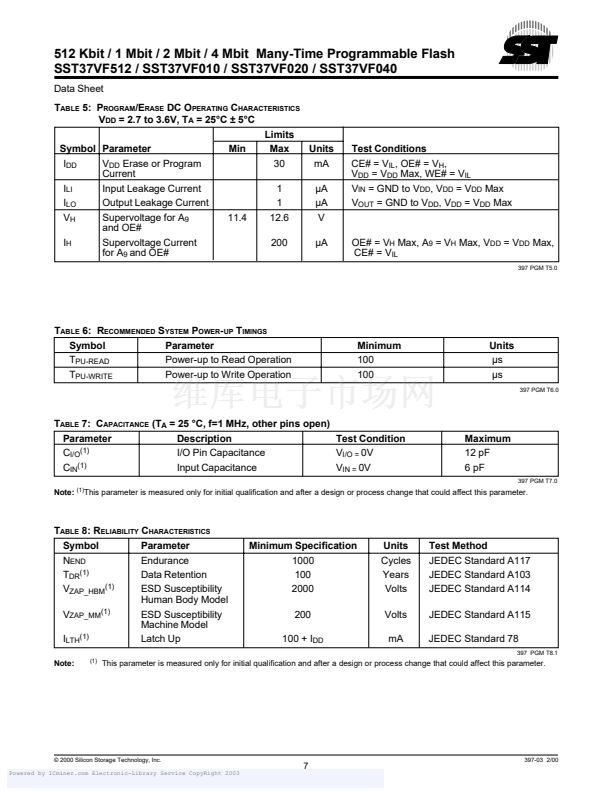
鈥?Endurance: At least 1000 Cycles
鈥?Greater than 100 years Data Retention
鈥?Low Power Consumption
鈥?Active Current: 10 mA (typical)
鈥?Standby Current: 1 碌A(chǔ) (typical)
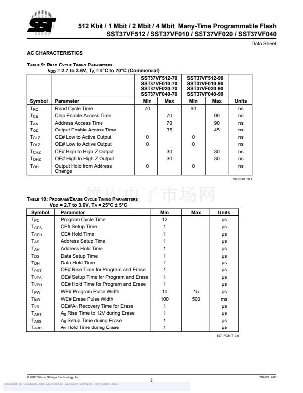
鈥?Fast Read Access Time
鈥?70 and 90 ns
鈥?Fast Byte-Program Operation
鈥?Byte-Program Time: 10 碌s (typical)
鈥?Chip-Program Time:
0.6 seconds (typical) for SST37VF512
1.2 seconds (typical) for SST37VF010
2.4 seconds (typical) for SST37VF020
4.8 seconds (typical) for SST37VF040
鈥?Electrical Erase Using Programmer
鈥?Does not require UV source
鈥?Chip-Erase Time: 100 ms (typical)
鈥?CMOS I/O Compatibility
鈥?JEDEC Standard Byte-wide Flash EEPROM
Pinouts
鈥?Packages Available
鈥?32-Pin PDIP
鈥?32-Pin PLCC
鈥?32-Pin TSOP (8mm x 14mm)
PRODUCT DESCRIPTION
The SST37VF512/010/020/040 devices are 64K x8 /
128K x8 / 256K x8 / 512K x8 CMOS, Many-Time Pro-
grammable (MTP), low cost flash, manufactured with
SST鈥檚 proprietary, high performance CMOS SuperFlash
technology. The split-gate cell design and thick oxide
tunneling injector attain better reliability and
manufacturability compared with alternate approaches.
The SST37VF512/010/020/040 can be electrically erased
and programmed at least 1000 times using an external
programmer, e.g., to change the contents of devices in
inventory. The SST37VF512/010/020/040 have to be
erased prior to programming. These devices conform to
JEDEC standard pinouts for byte-wide flash memories.
Featuring high performance Byte-Program, the
SST37VF512/010/020/040 provide a typical Byte-Pro-
gram time of 10 碌s. Designed, manufactured, and tested
for a wide spectrum of applications, these devices are
offered with an endurance of at least 1000 cycles. Data
retention is rated at greater than 100 years.
The SST37VF512/010/020/040 are suited for
applications that require infrequent writes and low
power nonvolatile storage. These devices will
improve flexibility, efficiency, and performance while
matching the low cost in nonvolatile applications that
currently use UV-EPROMs, OTPs, and mask ROMs.
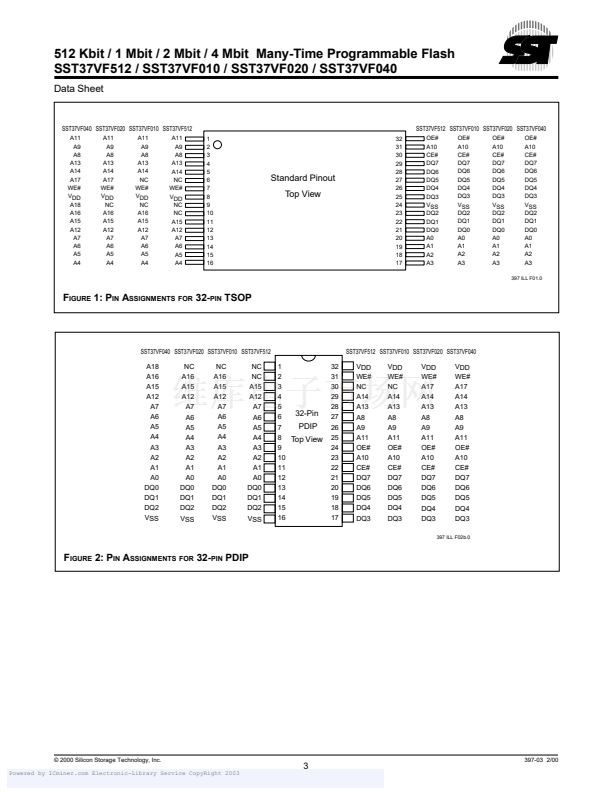
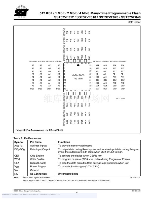
To meet surface mount and conventional through hole
requirements, the SST37VF512/010/020/040 are of-
fered in 32-pin PLCC, PDIP and TSOP packages. See
Figures 1, 2 and 3 for pinouts.
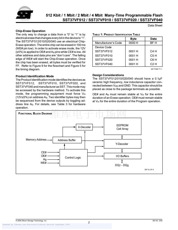
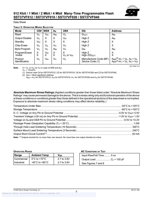
Device Operation
The SST37VF512/010/020/040 devices are nonvolatile
memory solutions that can be used instead of standard
flash devices if in-system programmability is not re-
quired. It is functionally (Read) and pin compatible with
industry standard flash products.The device supports
electrical Erase operation via an external programmer.
Read
The Read operation of the SST37VF512/010/020/040 is
controlled by CE# and OE#. Both CE# and OE# have to be
low for the system to obtain data from the outputs. Once the
address is stable, the address access time is equal to the
delay from CE# to output (T
CE
). Data is available at the
output after a delay of T
OE
from the falling edge of OE#,
assuming the CE# pin has been low and the addresses
have been stable for at least T
CE
- T
OE
. When the CE# pin
is high, the chip is deselected and a standby current of only
10 碌A(chǔ) (typical) is consumed. OE# is the output control and
is used to gate data from the output pins. The data bus is
in high impedance state when either CE# or OE# is V
IH
.
Refer to Figure 4 for the timing diagram.
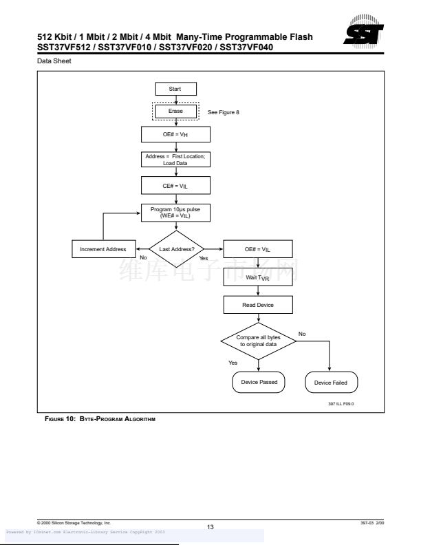
Byte-Program Operation
The SST37VF512/010/020/040 are programmed by us-
ing an external programmer. The programming mode is
activated by asserting 12V (鹵5%) on OE# pin and V
IL
on
CE# pin. The device is programmed using a single pulse
(WE# pin low) of 10 碌s per byte. Using the MTP program-
ming algorithm, the Byte-Program process continues
byte-by-byte until the entire chip has been programmed.
Refer to Figure 10 for the flowchart and Figure 6 for the
timing diagram.
1
2
3
4
5
6
7
8
9
10
11
12
13
14
15
16
漏 2000 Silicon Storage Technology, Inc.The SST logo and SuperFlash are registered trademarks of Silicon Storage Technology, Inc. MTP is a trademark of Silicon Storage Technology, Inc.
1
397-03 2/00
These specifications are subject to change without notice.
Powered by ICminer.com Electronic-Library Service CopyRight 2003


 1
1
 2
2
 3
3
 4
4
 5
5
 6
6
 7
7
 8
8
 9
9
 10
10
 11
11
 12
12
 13
13
 14
14
 15
15
 16
16
