4 Mbit ROM + 1 Mbit / 256 Kbit SRAM
ROM/RAM Combo
SST30VR041 / SST30VR043
SST30VR041 / 0434Mb Mask ROM (x8) + 1Mb / 256Kb SRAM (x8) Combo
Data Sheet
FEATURES:
鈥?ROM + SRAM ROM/RAM Combo
鈥?SST30VR041: 512K x8 ROM + 128K x8 SRAM
鈥?SST30VR043: 512K x8 ROM + 32K x8 SRAM
鈥?ROM/RAM combo on a monolithic chip
鈥?Equivalent ComboMemory (Flash + SRAM):
SST31LF041A for code development and
pre-production
鈥?Wide Operating Voltage Range: 2.7-3.3V
鈥?Chip Access Time
鈥?SST30VR041 70 ns and 150 ns
鈥?SST30VR043 150 ns
鈥?Low Power Dissipation:
鈥?Standby: 1.0 碌W (Typical)
鈥?Operating: 3.0 mW (Typical)
鈥?Fully Static Operation
鈥?No clock or refresh required
鈥?Three-state Outputs
鈥?Packages Available
鈥?32-lead TSOP (8mm x14mm)
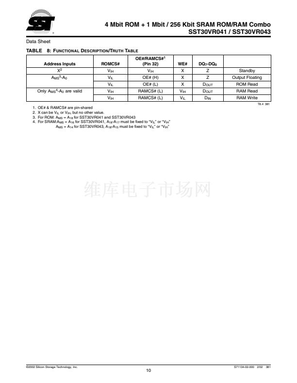
PRODUCT DESCRIPTION
The SST30VR041/043 are ROM/RAM combo chips
consisting of 4 Mbit Read-Only Memory (ROM) orga-
nized as 512 KByte and a Static Random Access
Memory (SRAM) organized as either 128 or 32 KByte.
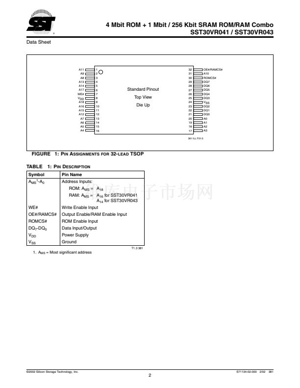
Output Enable Input (OE#) is pin-shared with
RAMCS# (RAM Enable Input) signal in order to main-
tain the standard 32-lead TSOP package.
The device is fabricated using SST鈥檚 advanced CMOS low
power process technology.
The SST30VR041/043 have an output enable input for pre-
cise control of the data outputs. It also has two (2) separate
chip enable inputs for selection of either SRAM or ROM
and for minimizing current drain during power-down mode.
The SST30VR041/043 is particularly well suited for use in
low voltage (2.7-3.3V) supplies such as pagers, organizers
and other handheld applications.
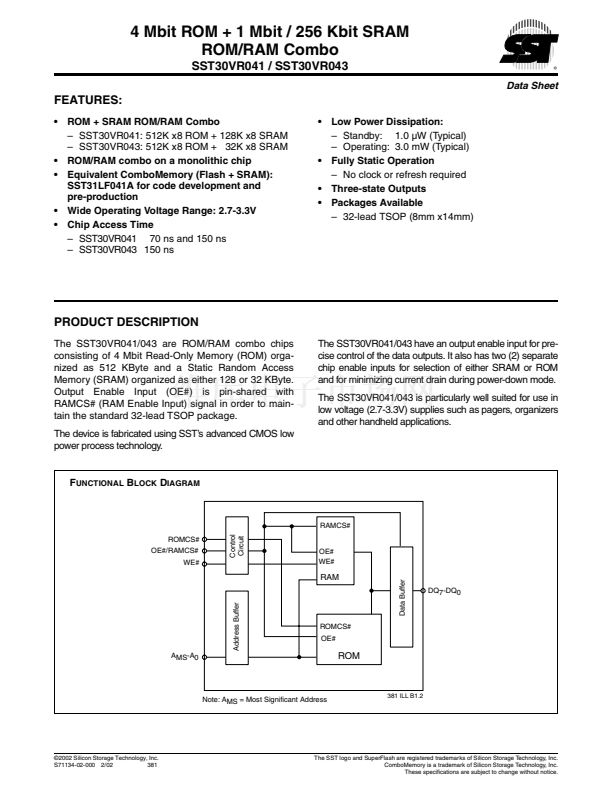
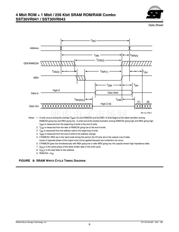
F
UNCTIONAL
B
LOCK
D
IAGRAM
RAMCS#
ROMCS#
OE#/RAMCS#
WE#
Control
Circuit
OE#
WE#
Data Buffer
RAM
Address Buffer
DQ7-DQ0
ROMCS#
OE#
AMS-A0
ROM
Note: AMS = Most Significant Address
381 ILL B1.2
漏2002 Silicon Storage Technology, Inc.
S71134-02-000 2/02
381
1
The SST logo and SuperFlash are registered trademarks of Silicon Storage Technology, Inc.
ComboMemory is a trademark of Silicon Storage Technology, Inc.
These specifications are subject to change without notice.


 1
1
 2
2
 3
3
 4
4
 5
5
 6
6
 7
7
 8
8
 9
9
 10
10
 11
11
 12
12
