鈻?/div>
Space Saving 10-Pin
碌SOIC
Package
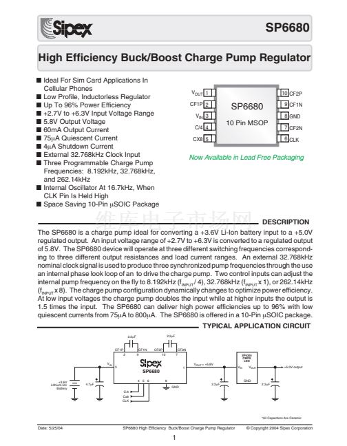
V
OUT
1
CF1P
2
V
IN
3
C/4
4
CX8
5
10
CF2P
SP6680
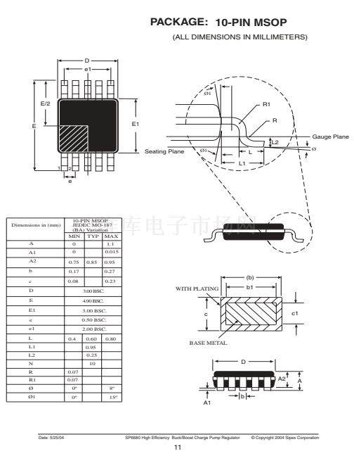
10 Pin MSOP
9
CF1N
8
GND
7
CF2N
6
CLK
Now Available in Lead Free Packaging
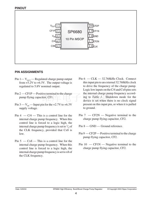
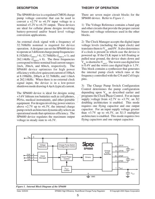
DESCRIPTION
The SP6680 is a charge pump ideal for converting a +3.6V Li-Ion battery input to a +5.0V
regulated output. An input voltage range of +2.7V to +6.3V is converted to a regulated output
of 5.8V. The SP6680 device will operate at three different switching frequencies correspond-
ing to three different output resistances and load current ranges. An external 32.768kHz
nominal clock signal is used to produce three synchronized pump frequencies through the use
an internal phase look loop of an to drive the charge pump. Two control inputs can adjust the
internal pump frequency on the fly to 8.192kHz (f
INPUT
/ 4), 32.768kHz (f
INPUT
x 1), or 262.14kHz
(f
INPUT
x 8). The charge pump configuration dynamically changes to optimize power efficiency.
At low input voltages the charge pump doubles the input while at higher inputs the output is
1.5 times the input. The SP6680 can deliver high power efficiencies up to 96% with low
quiescent currents from 75碌A(chǔ) to 800碌A(chǔ). The SP6680 is offered in a 10-Pin
碌SOIC
package.
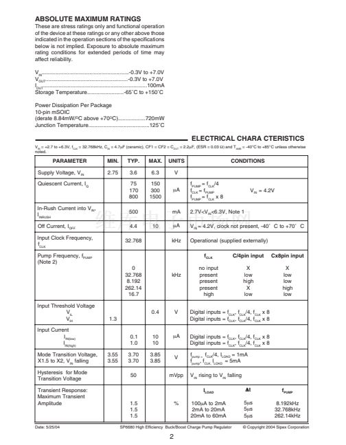
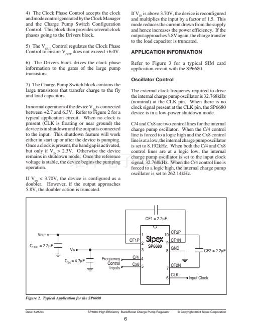
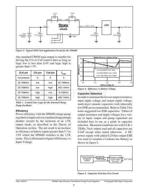
TYPICAL APPLICATION CIRCUIT
2.2碌F
2.2碌F
CF1P
2
V
IN
CF1N
9
CF2P
10
7
CF2N
SP6200
CMOS
LDO
3
1
V
OUT
= +5.8V
V
IN
SP6680
+3.6V
Lithium-Ion
Battery
4 5 6
4.7碌F
GND
C/4
Cx8
CLK
8
2.2碌F
V
OUT
+5.0V output
GND
2.2碌F
*All Capacitors Are Ceramic
Date: 5/25/04
SP6680 High Efficiency Buck/Boost Charge Pump Regulator
漏 Copyright 2004 Sipex Corporation
1


 1
1
 2
2
 3
3
 4
4
 5
5
 6
6
 7
7
 8
8
 9
9
 10
10
 11
11
 12
12
