廬
SP6660
200mA Charge Pump Inverter or Doubler
s
Inverts or Doubles Input Supply Voltage
s
93% Power Efficiency at 3.6V
s
10kHz/80kHz Selectable Oscillator
s
External Oscillator up to 700KHz
s
5鈩?Output Resistance at 3.6V
s
Low Voltage Battery Operation
s
Ideal for 3.6V Lithium Ion Battery
s
High Output Current 鈥?200mA
s
Pin-Compatible High-Current Upgrade of
the ICL7660 and 660 Industry Standard
s
Smallest Package Available for the 660
Industry Standard 鈥?8pin
碌SOIC
DESCRIPTION
The
SP6660
is a CMOS DC-DC Monolithic Voltage Converter that can be implemented as a
Voltage Inverter or a Positive Voltage Doubler. As a Voltage Inverter, a -1.5V to -4.25V output
can be converted from a +1.5V to +4.25V input. As a Voltage Doubler, the
SP6660
can provide
a +8.0V output at 100mA from a +4.25V input. The
SP6660
is ideal for both battery-powered
and board level voltage conversion applications with a typical operating current of 400碌A(chǔ) and
a high efficiency (>90%) over most of its load-current range. Typical end products for this
device are operational amplifier and interface power supplies, medical instruments, and hand-
held and laptop computers. The
SP6660
is available in 8-pin DIP, SOIC, and
碌SOIC
packages.
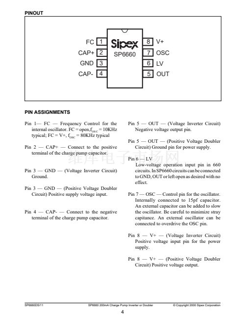
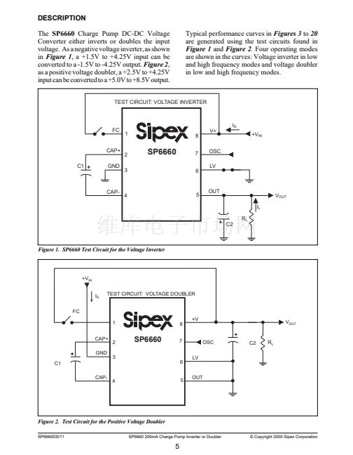
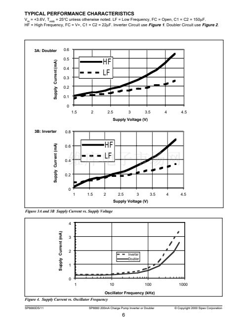
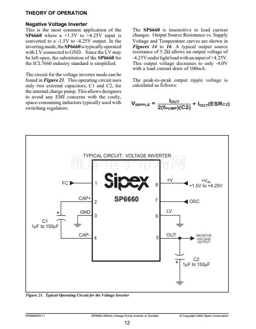
TYPICAL CIRCUIT: VOLTAGE INVERTER
+V
IN
+1.5V to +4.25V
TYPICAL CIRCUIT: VOLTAGE DOUBLER
FC
CAP+
GND
C1
1碌F to 150碌F
CAP-
1
+V
8
+V
IN
+1.5V to +4.25V
FC
1
CAP+
GND
+V
8
2
3
SP6660
7
LV
6
OSC
2
3
DOUBLE
VOLTAGE
OUTPUT
SP6660
7
LV
OSC
C2
1碌F to 150碌F
4
5
OUT
NEGATIVE
VOLTAGE
OUTPUT
C1
1碌F to 150碌F
CAP-
4
6
5
OUT
C2
1碌F to 150碌F
SP6660DS/11
SP6660 200mA Charge Pump Inverter or Doubler
漏 Copyright 2000 Sipex Corporation
1


 1
1
 2
2
 3
3
 4
4
 5
5
 6
6
 7
7
 8
8
 9
9
 10
10
 11
11
 12
12
 13
13
 14
14
 15
15
 16
16
 17
17
 18
18
 19
19
 20
20
 21
21
 22
22
