鈥?/div>
Page write
2.5 to 5.5 V
1.8 to 5.5 V
8 bytes (S-24C01A, S-24C02A)
16 bytes (S-24C04A)
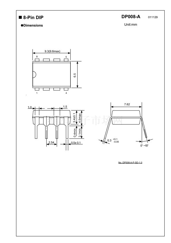
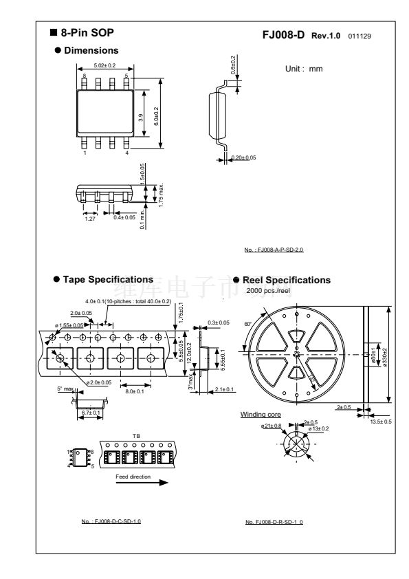
Package
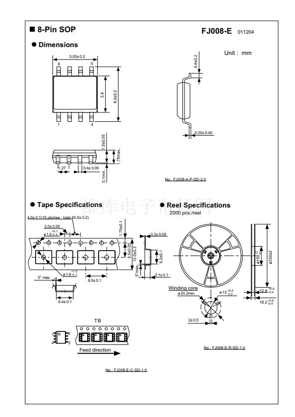
8-pin DIP
8-pin SOP
(PKG drawing code : DP008-A,DP008-C)
(PKG drawing code : FJ008-D,FJ008-E)
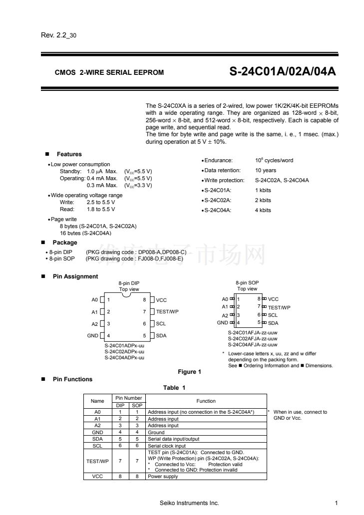
Pin Assignment
8-pin DIP
Top view
A0
A1
A2
GND
1
2
3
4
8
7
6
5
VCC
TEST/WP
SCL
SDA
A0
A1
A2
GND
8-pin SOP
Top view
1
2
3
4
8
7
6
5
VCC
TEST/WP
SCL
SDA
S-24C01ADPx-uu
S-24C02ADPx-uu
S-24C04ADPx-uu
S-24C01AFJA-zz-uuw
S-24C02AFJA-zz-uuw
S-24C04AFJA-zz-uuw
* Lower-case letters x, uu, zz and w differ
depending on the packing form.
See Ordering Information and Dimensions.
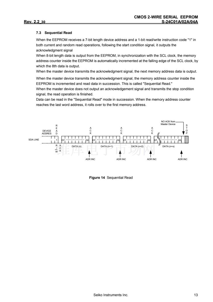
Figure 1
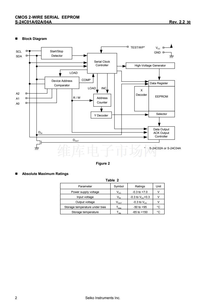
Pin Functions
Table 1
Name
A0
A1
A2
GND
SDA
SCL
TEST/WP
VCC
Pin Number
DIP
SOP
1
1
2
2
3
3
4
4
5
5
6
6
7
8
7
8
Function
Address input (no connection in the S-24C04A*)
Address input
Address input
Ground
Serial data input/output
Serial clock input
TEST pin (S-24C01A): Connected to GND.
WP (Write Protection) pin (S-24C02A, S-24C04A):
* Connected to Vcc:
Protection valid
* Connected to GND: Protection invalid
Power supply
* When in use, connect to
GND or Vcc.
Seiko Instruments Inc.
1


 1
1
 2
2
 3
3
 4
4
 5
5
 6
6
 7
7
 8
8
 9
9
 10
10
 11
11
 12
12
 13
13
 14
14
 15
15
 16
16
 17
17
 18
18
 19
19
 20
20
 21
21
 22
22
 23
23
