鈥?/div>
Adjustable rise and fall times
Adjustable output voltage swing
Short circuit protected
Output overvoltage protected
Sync and clock enable inputs
TTL and CMOS compatible inputs
MIL-STD-883B types available
100 Kbits/second data rate
Description
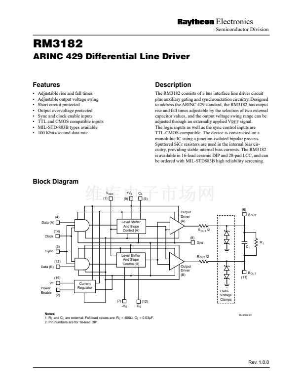
The RM3182 consists of a bus interface line driver circuit
plus auxiliary gating and synchronization circuitry. Designed
to address the ARINC 429 standard, the RM3182 has output
rise and fall times adjustable by the selection of two external
capacitor values, and the output voltage swing range can be
adjusted through an externally applied V
REF
signal.
The logic inputs as well as the sync control inputs are
TTL-CMOS compatible. The device is constructed on a
monolithic IC using a junction-isolated bipolar process.
Sputtered SiCr resistors are used in the internal bias cir-
cuitry, providing stable internal bias currents. The RM3182
is available in 16-lead ceramic DIP and 28-pad LCC, and can
be ordered with MIL-STD883B high reliability screening.
Block Diagram
V
REF
(1)
+V
S
(9)
C
A
(5)
(6)
A
OUT
(4)
Data (A)
(14)
Clock
(3)
Sync
(13)
Data (B)
(16)
V1
Power
Enable
Current
Regulator
(2)
(7)
-V
S
C
B
(12)
Level Shifter
And Slope
Control (B)
Level Shifter
And Slope
Control (A)
Output
Driver
(A)
R
OUT
/2
(8)
Gnd
R
L
C
L
R
OUT
/2
Output
Driver
(B)
B
OUT
(11)
Over-
Voltage
Clamps
Notes:
1. R
L
and C
L
are external. Full load values are: R
L
= 400鈩? C
L
= 0.03碌F.
2. Pin numbers are for 16-lead DIP.
65-3182-01
Rev. 1.0.0


 1
1
 2
2
 3
3
 4
4
 5
5
 6
6
 7
7
 8
8
