RFD12N06RLE, RFD12N06RLESM,
RFP12N06RLE
Data Sheet
January 2002
17A, 60V, 0.071 Ohm, N-Channel, Logic
Level UltraFET Power MOSFET
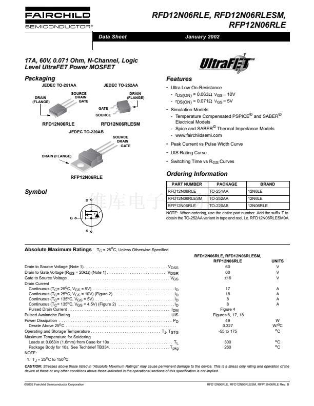
Packaging
JEDEC TO-251AA
DRAIN
(FLANGE)
SOURCE
DRAIN
GATE
GATE
SOURCE
Features
JEDEC TO-252AA
DRAIN
(FLANGE)
鈥?Ultra Low On-Resistance
- r
DS(ON)
= 0.063鈩?
V
GS
=
10V
- r
DS(ON)
= 0.071鈩?
V
GS
=
5V
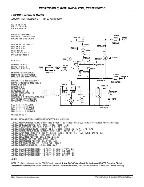
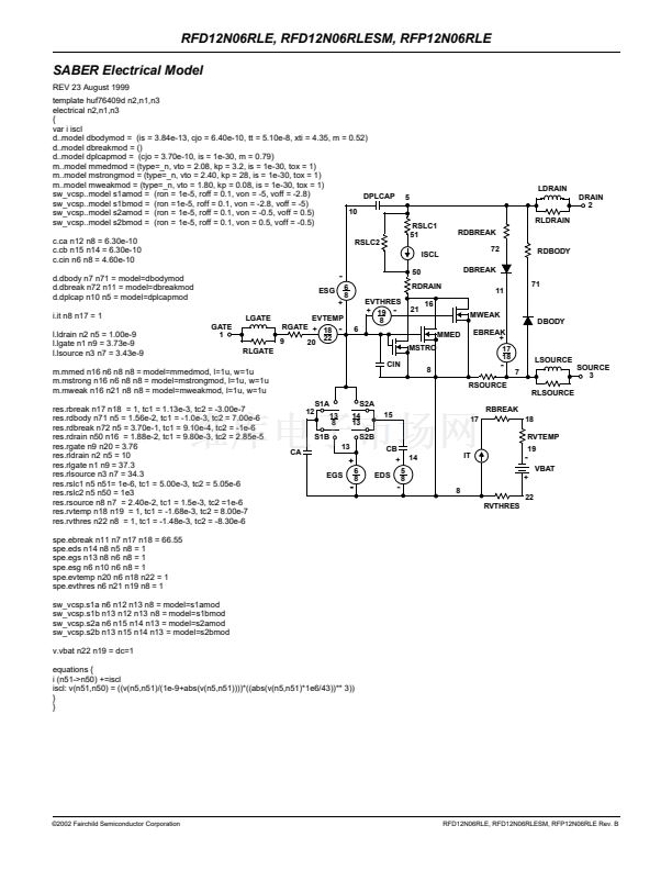
鈥?Simulation Models
- Temperature Compensated PSPICE
廬
and SABER
漏
Electrical Models
- Spice and SABER
漏
Thermal Impedance Models
- www.fairchildsemi.com
鈥?Peak Current vs Pulse Width Curve
鈥?UIS Rating Curve
鈥?Switching Time vs R
GS
Curves
RFD12N06RLE
RFD12N06RLESM
SOURCE
DRAIN
GATE
JEDEC TO-220AB
DRAIN (FLANGE)
RFP12N06RLE
Ordering Information
PART NUMBER
PACKAGE
TO-251AA
TO-252AA
TO-220AB
BRAND
12N6LE
12N6LE
12N06RLE
RFD12N06RLE
Symbol
D
RFD12N06RLESM
RFP12N06RLE
G
NOTE: When ordering, use the entire part number. Add the suffix T to
obtain the TO-252AA variant in tape and reel, i.e. RFD12N06RLESM9A.
S
Absolute Maximum Ratings
T
C
= 25
o
C, Unless Otherwise Specified
RFD12N06RLE, RFD12N06RLESM,
RFP12N06RLE
60
60
鹵16
17
18
8
8
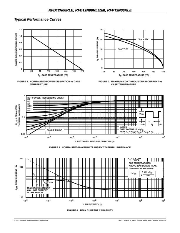
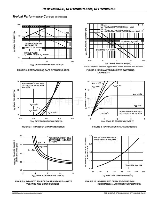
Figure 4
Figures 6, 17, 18
49
0.327
-55 to 175
300
260
UNITS
V
V
V
A
A
A
A
Drain to Source Voltage (Note 1) . . . . . . . . . . . . . . . . . . . . . . . . . . . . . . . . . . . . . V
DSS
Drain to Gate Voltage (R
GS
= 20k鈩? (Note 1) . . . . . . . . . . . . . . . . . . . . . . . . . . V
DGR
Gate to Source Voltage . . . . . . . . . . . . . . . . . . . . . . . . . . . . . . . . . . . . . . . . . . . . . V
GS
Drain Current
Continuous (T
C
= 25
o
C, V
GS
= 5V) . . . . . . . . . . . . . . . . . . . . . . . . . . . . . . . . . . . . I
D
Continuous (T
C
= 25
o
C, V
GS
= 10V) (Figure 2) . . . . . . . . . . . . . . . . . . . . . . . . . . . I
D
Continuous (T
C
= 135
o
C, V
GS
= 5V) . . . . . . . . . . . . . . . . . . . . . . . . . . . . . . . . . . . I
D
Continuous (T
C
= 135
o
C, V
GS
= 4.5V) (Figure 2) . . . . . . . . . . . . . . . . . . . . . . . . . I
D
Pulsed Drain Current . . . . . . . . . . . . . . . . . . . . . . . . . . . . . . . . . . . . . . . . . . . . . I
DM
Pulsed Avalanche Rating . . . . . . . . . . . . . . . . . . . . . . . . . . . . . . . . . . . . . . . . . . . UIS
Power Dissipation . . . . . . . . . . . . . . . . . . . . . . . . . . . . . . . . . . . . . . . . . . . . . . . . . . P
D
Derate Above 25
o
C . . . . . . . . . . . . . . . . . . . . . . . . . . . . . . . . . . . . . . . . . . . . . . . . .
Operating and Storage Temperature . . . . . . . . . . . . . . . . . . . . . . . . . . . . . . . T
J
, T
STG
Maximum Temperature for Soldering
Leads at 0.063in (1.6mm) from Case for 10s . . . . . . . . . . . . . . . . . . . . . . . . . . . . T
L
Package Body for 10s, See Techbrief TB334. . . . . . . . . . . . . . . . . . . . . . . . . . . T
pkg
NOTE:
1. T
J
= 25
o
C to 150
o
C.
W
W/
o
C
o
C
o
C
o
C
CAUTION:
Stresses above those listed in 鈥淎bsolute Maximum Ratings鈥?may cause permanent damage to the device. This is a stress only rating and operation of the
device at these or any other conditions above those indicated in the operational sections of this specification is not implied.
漏2002 Fairchild Semiconductor Corporation
RFD12N06RLE, RFD12N06RLESM, RFP12N06RLE Rev. B


 1
1
 2
2
 3
3
 4
4
 5
5
 6
6
 7
7
 8
8
 9
9
 10
10
