鈥?/div>
Eight zero delay outputs
Selectable positive or negative edge synchronization
Synchronous output enable
Output frequency: 25MHz to 85MHz
CMOS outputs
3 skew grades:
QS59920 -2: t
SKEW0
<250ps
QS59920 -5: t
SKEW0
<500ps
QS59920 -7: t
SKEW0
<750ps
3-level input for PLL range control
PLL bypass for DC testing
External feedback, internal loop filter
46mA I
OL
high drive outputs
Low Jitter: <200ps peak-to-peak
Outputs drive 50鈩?terminated lines
Pin compatible with Cypress CY7B9920
Available in SOIC Package
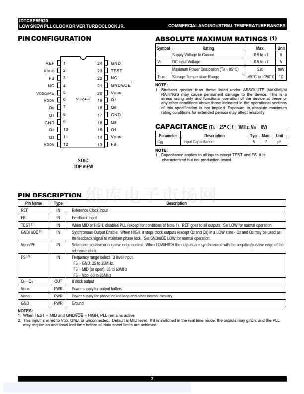
QS59920
DESCRIPTION:
The QS59920 is a high fanout phase lock loop clock driver intended
for high performance computing and data-communications applications.
The QS59920 has CMOS outputs.
The QS59920 maintains Cypress CY7B9920 compatibility while pro-
viding two additional features: Synchronous Output Enable (GND/sOE),
and Positive/Negative Edge Synchronization (V
DDQ
/PE). When the GND/
sOE
pin is held low, all outputs are synchronously enabled (CY7B9920
compatibility). However, if GND/sOE is held high, all outputs except Q2
and Q3 are synchronously disabled.
Furthermore, when the V
DDQ
/PE is held high, all outputs are syn-
chronized with the positive edge of the REF clock input (CY7B9920
compatibility). When V
DDQ
/PE is held low, all outputs are synchronized
with the negative edge of REF.
The FB signal is compared with the input REF signal at the phase
detector in order to drive the VCO. Phase differences cause the VCO
of the PLL to adjust upwards or downwards accordingly.
An internal loop filter moderates the response of the VCO to the
phase detector. The loop filter transfer function has been chosen to
provide minimal jitter (or frequency variation) while still providing accu-
rate responses to input frequency changes.
鈥?/div>
鈥?/div>
鈥?/div>
鈥?/div>
鈥?/div>
鈥?/div>
鈥?/div>
鈥?/div>
FUNCTIONAL BLOCK DIAGRAM
V
DDQ
/PE
GND/sOE
Q
0
Q
1
Q
2
Q
3
PLL
REF
Q
4
Q
5
FS
Q
6
Q
7
FB
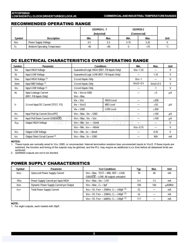
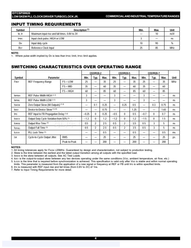
COMMERCIAL/INDUSTRIAL TEMPERATURE RANGES
1
c
1999
Integrated Device Technology, Inc.
MARCH 2000
DSC-5813/-
QS59920-5SOI相關(guān)型號(hào)PDF文件下載
-
型號(hào)
版本
描述
廠商
下載
-
英文版
LOW SKEW CMOS PLL CLOCK DRIVER WITH INTEGRATED LOOP FILTER
IDT
-
英文版
LOW SKEW CMOS PLL CLOCK DRIVER WITH INTEGRATED LOOP FILTER
IDT
-
英文版
LOW SKEW CMOS PLL CLOCK DRIVER WITH INTEGRATED LOOP FILTER
IDT [Integ...
-
英文版
LOW SKEW CMOS PLL CLOCK DRIVER WITH INTEGRATED LOOP FILTER
IDT
-
英文版
LOW SKEW CMOS PLL CLOCK DRIVER WITH INTEGRATED LOOP FILTER
IDT
-
英文版
LOW SKEW CMOS PLL CLOCK DRIVER WITH INTEGRATED LOOP FILTER
IDT
-
英文版
LOW SKEW CMOS PLL CLOCK DRIVER WITH INTEGRATED LOOP FILTER
IDT [Integ...
-
英文版
EIGHT DISTRIBUTED-OUTPUT CLOCK DRIVER|CMOS|LDCC|28PIN|PLASTI...
ETC
-
英文版
EIGHT DISTRIBUTED-OUTPUT CLOCK DRIVER|CMOS|SSOP|28PIN|PLASTI...
ETC
-
英文版
LOW SKEW TTL PLL CLOCK DRIVER WITH INTEGRATED LOOP FILTER
IDT
-
英文版
LOW SKEW TTL PLL CLOCK DRIVER WITH INTEGRATED LOOP FILTER
IDT [Integ...
-
英文版
Ten Distributed-Output Clock Driver
ETC
-
英文版
LOW SKEW CMOS PLL CLOCK DRIVER WITH INTEGRATED LOOP FILTER
IDT
-
英文版
LOW SKEW CMOS PLL CLOCK DRIVER WITH INTEGRATED LOOP FILTER
IDT [Integ...
-
英文版
SIX DISTRIBUTED-OUTPUT CLOCK DRIVER|CMOS|SSOP|20PIN|PLASTIC
ETC
-
英文版
LOW SKEW TTL PLL CLOCK DRIVER WITH INTEGRATED LOOP FILTER
IDT
-
英文版
Four Distributed-Output Clock Driver
ETC
-
英文版
EIGHT DISTRIBUTED-OUTPUT CLOCK DRIVER|CMOS|LDCC|28PIN|PLASTI...
ETC
-
英文版
EIGHT DISTRIBUTED-OUTPUT CLOCK DRIVER|CMOS|SSOP|28PIN|PLASTI...
ETC
-
英文版
Ten Distributed-Output Clock Driver
ETC


 1
1
 2
2
 3
3
 4
4
 5
5
 6
6
