鈥?/div>
5V operation
Six low noise CMOS level outputs
Q outputs, Q/2 output
<500ps output skew, Q
0
鈥換
4
Outputs 3-state and reset while OE/RST low
PLL disable feature for low frequency testing
Internal loop filter RC network
Internal VCO/2 option
Balanced drive outputs 鹵36mA
ESD >2000V
80MHz maximum frequency
Available in QSOP package
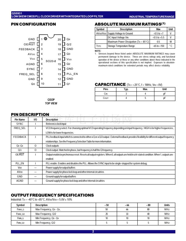
QS5931
DESCRIPTION:
The QS5931 Clock Driver uses an internal phase locked loop (PLL)
to lock low skew outputs to a reference clock input. Six outputs are
available: Q
0
鈥換
4
, Q/2. Careful layout and design ensure < 500ps
skew between the Q
0
鈥換
4
, and Q/2 outputs. The QS5931 includes an
internal RC filter which provides excellent jitter characteristics and
eliminates the need for external components. Various combinations of
feedback and a divide-by-2 in the VCO path allow applications to be
customized for linear VCO operation over a wide range of input SYNC
frequencies. The PLL can also be disabled by the PLL_EN signal to
allow low frequency or DC testing. The QS5931 is designed for use
in cost sensitive high-performance computing systems, workstations,
multi-board computers, networking hardware, and mainframe sys-
tems. Several can be used in parallel or scattered throughout a sys-
tem for guaranteed low skew, system-wide clock distribution networks.
In the QSOP package, the QS5931 clock driver represents the best
value in small form factor, high-performance clock management prod-
ucts.
For more information on PLL clock driver products, see Application
Note AN-227.
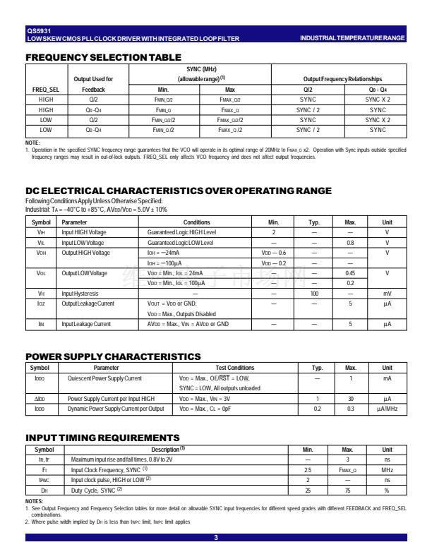
FUNCTIONAL BLOCK DIAGRAM
FEEDBACK
PLL_EN
FREQ _SEL
SYNC
O E/RST
PH ASE
DETECTO R
LOO P
FILTER
0
1
VCO
1
/2
0
R
D
R
D
R
D
R
D
R
D
R
D
Q
Q
Q
Q
Q
Q
Q
Q /2
Q
4
Q
3
Q
2
Q
1
Q
0
The IDT logo is a registered trademark of Integrated Device Technology, Inc.
INDUSTRIAL TEMPERATURE RANGE
1
c
2002
Integrated Device Technology, Inc.
JANUARY 2002
DSC-5817/2


 1
1
 2
2
 3
3
 4
4
 5
5
 6
6
 7
7
 8
8
