Phototransistors
PNZ120S
(PN120S)
Silicon NPN Phototransistor
Unit : mm
For optical control systems
4.1鹵0.3
2.0鹵0.2
12.5 min.
酶3.0鹵0.2
Can be combined with LN62S to form an optical controller
Features
High sensitivity
Wide directional sensitivity for easy use
Fast response : t
r
, t
f
= 3
碌s
(typ.)
Small size (酶 3) ceramic package
酶0.3鹵0.05
酶0.45鹵0.05
0.9鹵0.15
Absolute Maximum Ratings
(Ta = 25藲C)
Parameter
Collector to emitter voltage
Emitter to collector voltage
Collector current
Collector power dissipation
Operating ambient temperature
Storage temperature
Symbol
V
CEO
V
ECO
I
C
P
C
T
opr
T
stg
Ratings
30
5
20
50
鈥?5 to +85
鈥?0 to +100
Unit
V
V
mA
mW
藲C
藲C
2
1
1: Emitter
2: Collector
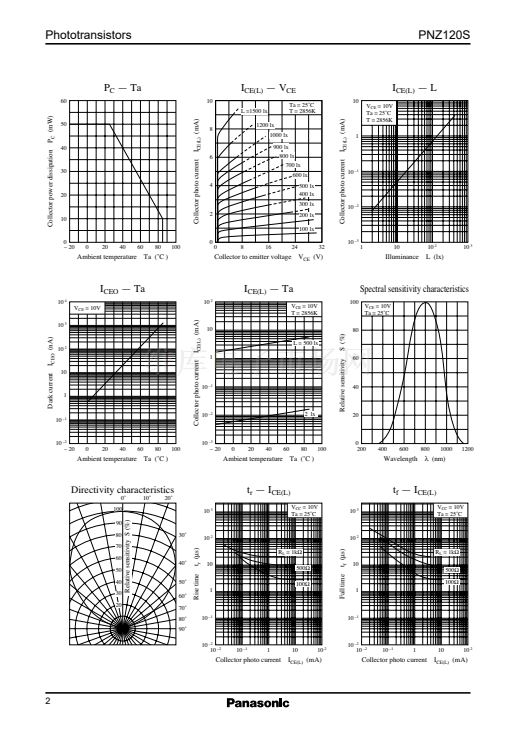
Electro-Optical Characteristics
(Ta = 25藲C)
Parameter
Dark current
Collector photo current
Peak sensitivity wavelength
Acceptance half angle
Response time
Collector saturation voltage
*1
*2
Symbol
I
CEO
I
CE(L)1
I
CE(L)2
位
P
胃
t
r
, t
f*2
V
CE(sat)
V
CE
= 10V
Conditions
V
CE
= 10V, L = 2 lx
*1
V
CE
= 10V, L = 500 lx
*1
V
CE
= 10V
Measured from the optical axis to the half power point
V
CC
= 10V, I
CE(L)
= 5mA, R
L
= 100鈩?/div>
I
CE(L)
= 1mA, L = 1000 lx
*1
min
3
typ
5
*3
*3
max
500
Unit
nA
碌A
mA
nm
deg.
碌s
800
50
3
0.2
0.5
V
Measurements were made using a tungsten lamp (color temperature T = 2856K) as a light source.
Switching time measurement circuit
Sig.IN
V
CC
(Input pulse)
Sig.OUT (Output pulse)
90%
10%
t
d
t
r
t
f
t
d
: Delay time
t
r
: Rise time (Time required for the collector photo current to
increase from 10% to 90% of its final value)
t
f
: Fall time (Time required for the collector photo current to
decrease from 90% to 10% of its initial value)
;;
;;
;;
*3
I
CE(L)
50鈩?/div>
R
L
Classifications
Class
I
CE(L)1
(碌A)
I
CE(L) 2
(mA)
QL
3 to 16
5 typ.
RL
10 to 30
6 typ.
SL
>24
8 typ.
Note) The part number in the parenthesis shows conventional part number.
1


 1
1
 2
2
 3
3
