21098765432121098765432109876543210987654321210987654321098765432109876543212109876543210987654321098765432121098765432109876543210987654321
21098765432121098765432109876543210987654321210987654321098765432109876543212109876543210987654321098765432121098765432109876543210987654321
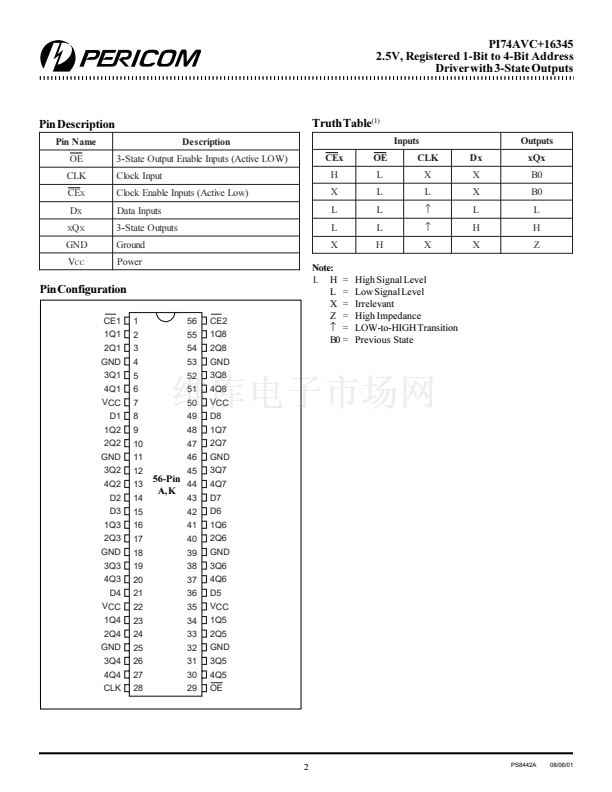
PI74AVC+16345
2.5V, Registered 1-Bit to 4-Bit Address
Driver w/3-State Outputs
Product Features
聲
PI74AVC+16345 is designed for low-voltage operation,
V
CC
= 1.65V to 3.6V
聲
True 鹵24mA Balanced Drive @3.3V
聲
I
OFF
supports partial power down operation
聲
I/O Tolerant to 3.6V
聲
All outputs contain a patented DDC
(Dynamic DriveControl) circuit that reduces noise without
degrading propagation delay.
聲
Industrial operation: 聳40擄C to +85擄C
聲
Available Packages:
聳 56-pin 240 mil wide plastic TSSOP (A)
聳 56-pin 173 mil wide plastic TVSOP (K)
Product Description
Pericom Semiconductor聮s PI74AVC+ series of logic circuits are
produced using the Company聮s advanced submicron CMOS
technology, achieving industry leading speed.
The PI74AVC+16345 is ideal for driving memory modules in
systems where multiple memory modules are used. One each of the
four output banks drive a different module; modules can be added
or removed without affecting the signal integrity of the other
modules in the system. Dual clock enables (CEx) allow use of the
device in high-speed memory interleaving applications where the
clock can be alternately enabled and disabled, allowing the address
to be held for additional cycles during memory access.
To ensure the high-impedance state during power up or power
down, OE should be tied to V
CC
through a pullup resistor; the
minimum value of the resistor is determined by the current sinking
capability of the driver.
Logic Block Diagram
1
CE1
29
OE
1Q1
D1
8
CE
D
56
CE2
1Q5
D5
36
CE
D
4Q1
4Q5
1Q2
D2
14
CE
D
1Q6
D6
42
CE
D
4Q2
4Q6
1Q3
D3
15
CE
D
1Q7
D7
43
CE
D
4Q3
4Q7
1Q4
D4
21
CE
D
1Q8
D8
49
CE
D
4Q4
CLK
28
4Q8
1
PS8442A
08/06/01


 1
1
 2
2
 3
3
 4
4
 5
5
 6
6
 7
7
 8
8
 9
9
 10
10
