21098765432121098765432109876543210987654321210987654321098765432109876543212109876543210987654321098765432121098765432109876543210987654321
21098765432121098765432109876543210987654321210987654321098765432109876543212109876543210987654321098765432121098765432109876543210987654321
PI74AVC+16334
2.5V 16-Bit Universal Bus Driver
with 3-State Outputs
Product Features
聲 PI74AVC+16334 is designed for low voltage operation,
V
CC
= 1.65V to 3.6V
聲 True 鹵24mA Balanced Drive @ 3.3V
聲 Compatible with Philips and T.I. AVC Logic family
聲 I
OFF
supports partial power-down operation
聲 3.6V I/O Tolerant inputs and outputs
聲 Meets PC133 SDRAM Registered DIMM specifications
聲 All outputs contain a patented DDC
(Dynamic Drive Control) circuit that reduces noise
without degrading propagation delay
聲 Industrial operation at 聳40擄C to +85擄C
聲 Available Packages:
聳 48-pin 240-mil wide plastic TSSOP (A)
聳 48-pin 173-mil wide plastic TVSOP (K)
Product Description
Pericom Semiconductor聮s PI74AVC+ series of logic circuits are
produced using the Company聮s advanced submicron CMOS
technology, achieving industry leading speed.
The 16-bit PI74AVC+16334 universal bus driver is designed
for 2.3V to 3.6V Vcc operation.
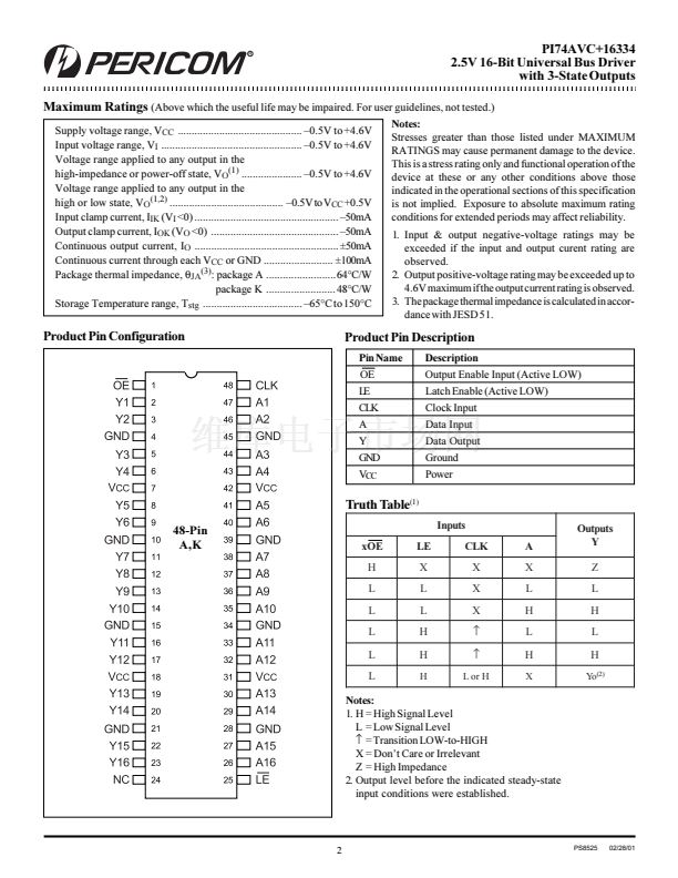
Data flow from A to Y is controlled by Output Enable (OE).
The device operates in the transparent mode when LE is LOW.
When LE is HIGH, the A data is latched if CLK is held at a high or
low logic level. If LE is HIGH, the A-data is stored in the latch/flip-
flop on the low-to-high transition of CLK. When OE is HIGH, the
outputs are in the high-impedance state.
To ensure the high-impedance state during power up or power down,
OE should be tied to Vcc through a pullup resistor; the minimum
value of the resistor is determined by the current-sinking capability
of the driver.
Logic Block Diagram
OE
CLK
LE
A1
1
48
25
47
1D
C1
CLK
2
Y1
TO 15 OTHER CHANNELS
1
PS8525
02/28/01


 1
1
 2
2
 3
3
 4
4
 5
5
 6
6
 7
7
 8
8
 9
9
 10
10
