21098765432121098765432109876543210987654321210987654321098765432109876543212109876543210987654321098765432121098765432109876543210987654321
21098765432121098765432109876543210987654321210987654321098765432109876543212109876543210987654321098765432121098765432109876543210987654321
PI74ALVTC16373
16-Bit Transparent D-Type Latch
with 3-STATE Outputs
Product Features
聲 PI74ALVTC family is designed for low voltage operation,
V
DD
= 1.8V to 3.6V
聲 Supports Live Insertion
聲 3.6V I/O Tolerant Inputs and Outputs
聲 Bus Hold
聲 High Drive, -32/64mA @ 3.3V
聲 Uses patented noise reduction circuitry
聲 Power-off high impedance inputs and outputs
聲 Industrial operation at 聳40擄C to +85擄C
聲 Packages available:
聳 48-pin 240 mil wide plastic TSSOP (A)
聳 48-pin 173 mil wide plastic TVSOP (K)
聳 48-pin 300 mil wide plastic SSOP (V)
Product Description
Pericom Semiconductor聮s PI74ALVTC series of logic circuits are
produced in the Company聮s advanced 0.35 micron CMOS
technology, achieving industry leading speed.
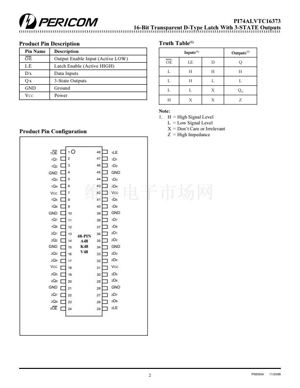
The PI74ALVTC16373 is particularly suitable for implementing
buffer registers, I/O ports, bidirectional bus drivers, and working
registers. This device can be used as two 8-bit latches or one 16-bit
latch. When the Latch Enable (LE) input is HIGH, the Q outputs
follow the (D) inputs. When LE is taken LOW, the Q outputs are
latched at the levels set up at the D inputs.
A buffered Output Enable (OE) input can be used to place the eight
outputs in either a normal logic state (high or low logic levels) or
a high-impedance state in which the outputs neither load nor drive
the bus lines significantly. The high-impedance state and the
increased drive provide the capability to drive bus lines without an
interface or pullup components. OE does not affect internal
operations of the latch. Old data can be retained or new data can be
entered while the ouputs are in the high-impedance state.
To ensure the high-impedance state during power up or power
down, OE should be tied to Vdd through a pullup resistor; the
minimum value of the resistor is determined by the current-sinking
capability of the driver.
The family offers both I/O Tolerant, which allows it to operate in
mixed 1.8/3.6V systems, and 聯(lián)Bus Hold,聰 which retains the data
input聮s last state whenever the data input goes to high-impedance,
preventing 聯(lián)floating聰 inputs and eliminating the need for pullup/
down resistors.
Logic Block Diagram
1OE
1
1LE
48
C1
2
1Q1
1D1
47
1D
To Seven Other Channels
24
2OE
2LE
25
C1
13
2Q1
2D1
36
1D
To Seven Other Channels
1
PS8355A
11/23/98


 1
1
 2
2
 3
3
 4
4
 5
5
 6
6
 7
7
 8
8
