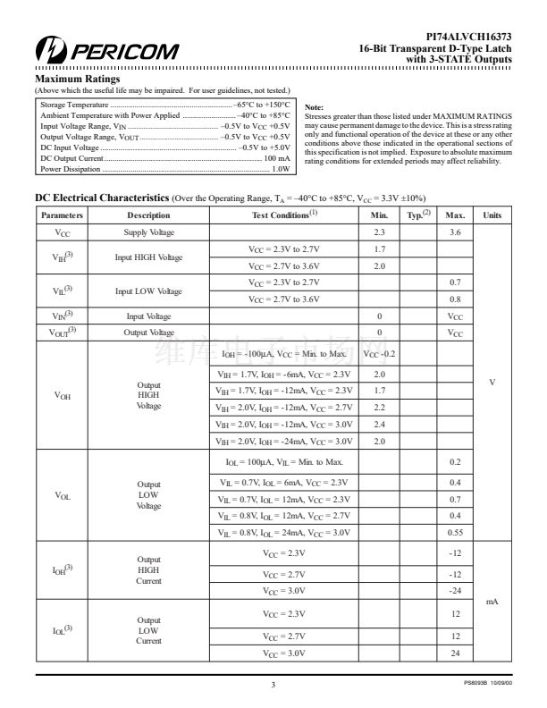
鈥?/div>
PI74ALVCH16373 is designed for low voltage operation
V
CC
= 2.3V to 3.6V
Hysteresis on all inputs
Typical V
OLP
(Output Ground Bounce)
< 0.8V at V
CC
= 3.3V, T
A
= 25擄C
Typical V
OHV
(Output V
OH
Undershoot)
< 2.0V at V
CC
= 3.3V, T
A
= 25擄C
Bus Hold retains last active bus state during 3-STATE,
eliminating the need for external pullup resistors
Industrial operation at 鈥?0擄C to +85擄C
Packages available:
鈥?48-pin 240 mil wide plastic TSSOP (A)
鈥?48-pin 300 mil wide plastic SSOP (V)
Product Description
Pericom Semiconductor鈥檚 PI74ALVCH series of logic circuits are
produced in the Company鈥檚 advanced 0.5 micron CMOS
technology, achieving industry leading speed.
This 16-bit transparent D-type latch is designed for 2.3V to 3.6V
V
CC
operation.
The PI74ALVCH16373 is particularly suitable for implementing
buffer registers, I/O ports, bidirectional bus drivers, and working
registers. This device can be used as two 8-bit latches or one 16-bit
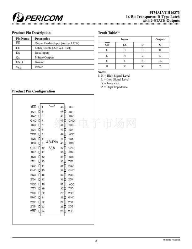
latch. When the Latch Enable (LE) input is HIGH, the Q outputs
follow the (D) inputs. When LE is taken LOW, the Q outputs are
latched at the levels set up at the D inputs.
A buffered Output Enable (OE) input can be used to place the
eight outputs in either a normal logic state (high or low logic
levels) or a high-impedance state in which the outputs neither
load nor drive the bus lines significantly. The high-impedance state
and the increased drive provide the capability to drive bus lines
without need for interface or pullup components. OE does not
affect internal operations of the latch. Old data can be retained
or new data can be entered while the outputs are in the high
impedance state.
To ensure the high impedance state during power up or power
down, OE should be tied to V
CC
through a pullup resistor; the
minimum value of the resistor is determined by the current-sinking
capability of the driver.
2
Logic Block Diagram
1OE
1
1LE
48
C1
1Q1
1D1
47
1D
Active bus-hold circuitry is provided to hold unused or floating
data inputs at a valid logic level.
To Seven Other Channels
24
2OE
2LE
25
C1
13
2Q1
2D1
36
1D
To Seven Other Channels
1
PS8093B 10/09/00


 1
1
 2
2
 3
3
 4
4
 5
5
