鈥?/div>
PI74ALVCH16260 is designed for low voltage operation
V
CC
= 2.3V to 3.6V
Hysteresis on all inputs
Typical V
OLP
(Output Ground Bounce)
< 0.8V at V
CC
= 3.3V, T
A
= 25擄C
Typical V
OHV
(Output V
OH
Undershoot)
< 2.0V at V
CC
= 3.3V, T
A
= 25擄C
Bus Hold retains last active bus state during 3-State,
eliminating the need for external pullup resistors
Industrial operation at 聳40擄C to +85擄C
Packages available:
聳 56-pin 240 mil wide plastic TSSOP (A)
聳 56-pin 300 mil wide plastic SSOP (V)
Pericom Semiconductor聮s PI74ALVCH series of logic circuits are
produced using the Company聮s advanced 0.5 micron CMOS
technology, achieving industry leading speed.
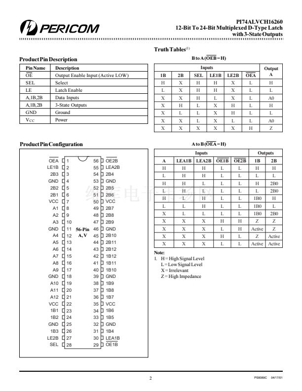
The PI74ALVCH16260 is a 12-bit to 24-bit multiplexed D-type latch
designed for 2.3V to 3.6 V
CC
operation. It is used in applications
where two separate datapaths must be multiplexed onto, or
demultiplexed from, a single data path.
Typical applications include multiplexing and/or demultiplexing
address and data information in microprocessor or bus-interface
and in memory-interleaving.
Three 12-bit I/O ports (A1-A12, 1B1-1B12, and 2B1-2B12) are available
for address and/or data transfer. The output-enable (OE1B, OE2B,
and OEA) inputs control bus transceiver functions. The OE1B and
OE2B control signals also allow bank control in the A-to-B direction.
Address and/or data information can be stored using the internal
storage latches. The latch-enable (LE1B, LE2B, LEA1B, and LEA2B)
inputs are used to control data storage. When the latch-enable input
is HIGH, the latch is transparent. When the latch-enable input goes
LOW, the data present at the inputs is latched and remains latched
until the latch-enable input is returned HIGH.
To ensure high-impedance state during power up or power down,
OE should be tied to V
CC
through a pullup resistor whose minimum
value is determined by the current-sinking capability of the driver.
Logic Block Diagram
LE1B
2
LE2B
27
30
LEA1B
LEA2B
55
OE2B
OE1B
OEA
56
29
Active bus-hold circuitry is provided to hold unused or floating
data inputs at a valid logic level.
1
SEL
28
G1
A1
8
C1
1
1
C1
1D
C1
1D
6
2B1
23
1D
1B1
C1
1D
TO 11 OTHER CHANNELS
1
PS8089C
04/17/01


 1
1
 2
2
 3
3
 4
4
 5
5
